- • Dr. Jarosław Domagała, Dr. Elżbieta Dynowska, and Dr. Roman Minikayev – Task 2.2 - Visit to ESRF, Grenoble, France
In the framework of task 2.2 of work package "Enhancing of human potential through exchange of know-how and twinning activities with partnering organization" Dr. Jarosław Domagała, Dr. Elżbieta Dynowska, and Dr. Roman Minikayev visited ESRF, Grenoble, France, in August 29th - September 3rd, 2016.
Firstly, the results obtained at the beamline ID-03 by Dr. Jankowski during spring 2016 were discussed. They came out as a result of a common project with group of applied crystallography from the Institute of Physics, Polish Academy of Sciences. These results served as a playground to learn the software written in the ESRF for the processing of the experimental data from two-dimensional detector (Binocular - to visualize reciprocal space maps and Pymca - to plot individual diffraction curves). The publication about new structure observed in ZnO implanted with Co similar to that of misfit-layered cobaltites is in preparation.
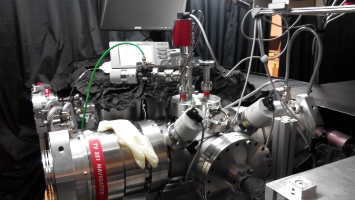
 Dr. Maciej Jankowski also explained in detail the operation of each element of the experimental line ID-03: optical hutch with monochromators (micrometer size beam of 1012 ph/s) and two large hutches hosting one vertical and one horizontal geometry diffractometers allowing SD studies in many different conditions.
Another part of the visit was dedicated to discussions on practical steps to prepare samples (ZnO layer implanted with varying dose of Co ions and annealed at different temperatures) as well as on measurements strategy for common project accepted at the SD line at January 2017.
Further cooperation in the field of the characterization of thin, nanometric size (Ga,Mn)As layers with different content of Mn and annealed at high temperatures by SD was discussed. The joint research project is planned to be submitted to the next beamtime from March to July 2017.
- • Dr. Ryszard Sobierajski – Task 2.14 - Visit to Eu-XFEL, Hamburg, Germany
In the framework of task 2.14 of work package "Enhancing of human potential through exchange of know-how and twinning activities with partnering organization" Dr. Ryszard Sobierajski visited Eu-XFEL, Hamburg, Germany, in August 22nd - 26th, 2016.
During my stay at Eu-XFEL facility I visited the SPB/SFX (Single Particles, clusters, and Biomolecules and Serial Femtosecond Crystallography), MID (Materials Imaging and Dynamics), HED (High Energy Density), and FXE (Femtosecond X-ray Experiments) experimental stations under construction at Eu-XFEL. I have learned about the necessary technical and electronic infrastructure. I’ve got familiar with the recent progress in the construction and first planned experiments. I met leading scientists responsible for the above listed stations and discussed with them the initiative of the Polish scientific community (supervised by IF PAN) regarding the scientific research at Eu-EXFEL.
Furthermore I presented to dr Peter Zalden the joined proposal for the PETRA synchrotron facility “Crystallization kinetics of metallic glasses via femtosecond laser heating”. We discussed the scientific scope of the proposal and the required instrumentation. It was agreed to use the X-ray diffraction and X-ray scattering techniques for the investigations of crystallisation kinetics of glasses.
Finally I discussed with Dr. Harald Sinn (Eu-XFEL) and Dr. Kai Tiedtke (DESY) the continuation of the joined experimental studies of the XFEL optics radiation hardness, in particular in the case of the cw-mode of operations.
- • MSc. Michał Grzybowski – Task 2.11 - Visit to University of Nottingham, UK
In the framework of task 2.11 of work package "Enhancing of human potential through exchange of know-how and twinning activities with partnering organization" MSc. Michał Grzybowski visited University of Nottingham, UK in August 18th - September 1st, 2016.
 During the visit, the work on the publication, concerning X-ray magnetic linear dichroism with photoemission electron microscopy detection (PEEM-XMLD) studies of CuMnAs done in collaboration between Institute of Physics Polish Academy of Sciences (IFPAN) and University of Nottingham (UoN), has been finalised. The visitor familiarized with the most recent advances in technology of antiferromagnetic CuMnAs growth and devices fabrication as well as the latest results in the PEEM-XMLD studies of thin layers of CuMnAs. The domain pattern dependence on the thickness and substrate were discussed.
The plan of the future collaboration between two institutions was made. The pioneering work in studies of the single antiferromagnetic domain CuMnAs devices and antiferromagnetic domain walls behaviour in the presence of Néel-order spin orbit torques were the key point of the discussions. Several scenarios of the possible structures of the devices were considered. The example is shown in the picture. Possible difficulties were taken into account. The devices will be fabricated at IFPAN using electron-beam lithography. They will be smaller than structures used previously in PEEM-XMLD studies of CuMnAs. The visit allowed to form a detailed plan of the collaboration between IFPAN and UoN in terms of antiferromagnetic materials studies for the incoming months.
- • Prof. Dr. hab. Maciej Sawicki – Task 2.16 - Visit to HZDR Helmholtz Centrum Dresden Rossendorf Institute of Ion Beam Physics and Materials Research, Dresden, Germany
In the framework of task 2.16 of work package "Enhancing of human potential through exchange of know-how and twinning activities with partnering organization" Prof. Dr. hab. Maciej Sawicki visited ZDR, Dresden, Germany in August 8th - 16th, 2016.
In the last decade, ion implantation combined with pulsed laser melting (PLM) has proved successful in achieving Mn-doped III-V dilute magnetic semiconductors such as (Ga,Mn)As, (In,Mn)As, and particularly (Ga,Mn)P and (In,Mn)P which pose a formidable challenge to be grown by “conventional” low-temperature molecular beam epitaxy. The collaboration IFPAN – HZDR in this field has recently been extended to nitrides – first layers of Mn implanted GaN has been obtained during the previous twinning visit of Prof. Sawicki to HZDR.
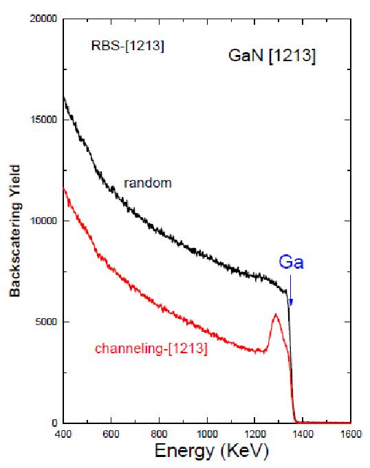 During this visit numerous meeting with Dr S. Prucnal and Dr S. Zhou were held to discuss the current state of the research in this field. Among many subject debated the most vividly were discussed results of magnetic measurements obtained for Mn implanted GaN, which gave purely isotropic response at low temperatures – indicating that Mn ions assume exclusively Mn2+ charge state after implantation. This in turn indicates either a presence of numerous donor-like points defects introduced in GaN during the irradiation or exclusively interstitial position of Mn ions within GaN host lattice. To resolve the issue Rutherford backscattering/channelling (RBS/C) analyses using 1.7 MeV, 4He+ ions were carried out to determine the damage profiles and the lattice site location of the implanted Mn. The measurements were performed at the HZDR campus with an active participation of prof. Sawicki. The analysis of the RBS/C results showed that the post-implantation flash lamp annealing has removed most of the implantation-induced damage. However, the damage recovery is not complete, since the channelling spectrum after the annealing does not return to the yield level of the virgin sample, indicating that better annealing parameters may be needed to eradicate the implantation damage completely. Combining the RBS/C with PIXE measurement it was established that that above 80% of the implanted Mn atoms occupy Ga lattice site after the Flash lamp annealing – calling for a further adjustment of the flash annealing stimulated regrowth of the implanted layer. Such attempts are planned for the next visit to HZDR.
Apart from this experimental activity a great deal of time was devoted to further refinements of two joint publications describing the work done on (Ga,Mn)As, (In, Mn)As and (In,Fe)As. Such a publication effort should certainly help to promote the research carried by both groups in view of prospects for joint projects. Also various technical issues and details of the currently employed experimental routines were discussed.
- • Prof. Dr. hab. Lech T. Baczewski – Task 2.16 - Visit to HZDR Helmholtz Centrum Dresden Rossendorf Institute of Ion Beam Physics and Materials Research, Dresden, Germany
In the framework of task 2.16 of work package "Enhancing of human potential through exchange of know-how and twinning activities with partnering organization" Prof. Dr. hab. Lech T. Baczewski visited ZDR, Dresden, Germany in August 3rd - 10th, 2016.
The aim of the visit was to to gain knowledge about the application of ion beam irradiation of thin solid films and nanostructures grown by MBE method allowing the tailoring of their structural and magnetic properties including nano-patterning and review of obtained results in view of common publication.
The Ion Beam Centre in HZDR provides experimental facilities with all kinds of ion beams, i. e. highly accelerated charged particles, in a broad energy range for the compositional analysis of materials and the modification of materials properties either by doping or by radiation damage and its personnel has a long lasting experience in such kind of techniques. The research aiming towards potential applications in nanoelectronics, optoelectronics, spintronics, and photovoltaics are of particular interest.
During the visit in HZDR detailed discussions took place with prof J. Fassbender – Director of the Institute for Materials Science, Dr Potzger – a group leader, Dr R. Bali and Dr. E. Josten – both post-docs in the lab. Different aspects related to ion irradiation of metallic thin films were discussed and explained how to use efficiently the TRIDYN software allowing to see the effects of ion irradiation in a specific thin film sample. This is important in order to plan correctly the sample configuration before the irradiation from the point of view of ion penetration depths, the precise ion dose determination.
Common results on GaAs nanorods and nanotubes covered by a ferromagnetic metal such as Co performed during the visits in IFPAN of HZDR scientists were reviewed and discussed. Ferromagnetic resonance (FMR) and Brillouin Light Scattering (BLS) were already performed on the samples prepared in IFPAN and further experiments are in progress. A draft version of common publication was discussed.
The proper way to prepare of beam-time application forms was also discussed as it is a very important issue increasing the success rate when applying for large facilities experiments for ion beam irradiation. Future use of ion beam facility in HZDR by scientists from IFPAN was planned. Reciprocally, a further collaboration regarding MBE grown samples preparation for common experiments is also envisaged.
The main outcomes of the visit are: (i) The extended knowledge about ion irradiation method and related effects in metallic thin films has been gained; (ii) Perspective of common projects was set; (iii) New characterisation techniques which can give a deeper insight into structural details of metallic nanostructures and interface magnetism origin were defined; (iv) Publication of common results was discussed; (v) Future collaboration scheme was established including the aspects of ion beam irradiation facility use in HZDR by Polish scientists and possibility of metallic nanostructures growth by MBE method in IFPAN for HZDR scientists for common research topics.
- • Dr. Grzegorz Łuka – Task 2.16 - Visit to HZDR Helmholtz Centrum Dresden Rossendorf Institute of Ion Beam Physics and Materials Research, Dresden, Germany
In the framework of task 2.16 of work package "Enhancing of human potential through exchange of know-how and twinning activities with partnering organization" Dr. Grzegorz Łuka visited HZDR Helmholtz Centrum Dresden Rossendorf Institute of Ion Beam Physics and Materials Research, Dresden, Germany, between July 31st – August 24th, 2016.
During the visit at the HZDR Helmholtz Centrum Dr. Łuka developed his skills in photoluminescence (PL) measurements. To this end Dr. Łuka investigated PL properties of undoped zinc oxide (ZnO) films grown by atomic layer deposition (ALD). ZnO films were grown by ALD at various growth temperatures (100 °C, 110 °C, 130 °C, 160 °C, and 200 °C) on SiO2/Si substrates. After deposition, the samples from each deposition process were annealed in air for 2 hours at four different temperatures (200 °C, 300 °C, 400 °C, and 500 °C). One sample from each growth process remained non annealed. The aim of the investigations was to identify differences in photoluminescence properties of the as-grown and annealed ZnO films and to assign those differences to the changes of the point defect structure and electrical properties of the films as a function of the processing conditions. Room temperature PL spectra were carried out for all 25 ZnO samples (5 growth temperatures × 5 processing conditions). Temperature dependent PL measurements were performed for six samples, i.e. five as grown ones + one sample grown at 100 °C and annealed at 200 °C.
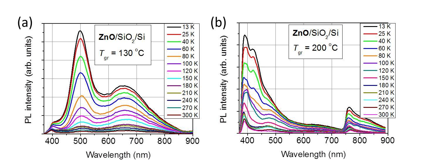
Fig. 1. Temperature dependent PL spectra of ZnO films grown by ALD at (a) 130°C and (b) at 200°C.
Fig. 1 shows temperature-dependent PL spectra of two ZnO layers, grown at different temperatures. The films grown at lower growth temperature, 130 °C (Fig. 1 a), show a high defect-related PL band centred at ~500 nm (~2.5 eV) and an additional band located at ~650 nm (~1.9 eV). A near-band edge emission (λ<400 nm) is very low. On the contrary, the films grown at 200 °C (Fig. 1 b) reveal higher band edge emission and defect related one located at ~430 nm (2.9 eV). The observed changes between the defect-related PL of the layers are therefore associated with a decrease of the concentration of acceptor defects like excess oxygen and zinc vacancies in favour of donor defects like zinc interstitials and oxygen vacancies.
- • Dr. hab. Hanka Przybylińska – Task 2.6 - Visit to University of Wuerzburg
In the framework of task 2.6 of work package "Enhancing of human potential through exchange of know-how and twinning activities with partnering organization" Dr. hab. Hanka Przybylińska visited University of Wuerzburg between July 24th – 29th, 2016.
Germanium telluride is one of the few simple ferroelectrics with only two ions per primitive cell. GeTe can be also easily doped with manganese, with solubility up to 50 %, without affecting the crystalline quality. (Ge,Mn)Te exhibits hole-mediated ferromagnetism, with transition temperature above 150 K for xMn around 0.5, which is among the highest Curie temperatures of all ferromagnetic semiconductors. However, high free carrier concentration (in excess of 1020 cm-3) necessary to induce ferromagnetic order prevents at the same time direct demonstration of ferroelectricity. The studies are performed with cooperation of JKU University in Linz, another EAgLE Partnering Organisation, where the layers are grown and structurally investigated.
During the visit many discussion were held to establish the best experimental protocol for this material. In particular, it was suggested to employ the ferromagnetic resonance (FMR) technique to investigate in detail the magnetocrystalline anisotropy experienced by Mn ions and hence use Mn as a sensor of the electric dipole moment. Some other topics were related to the influence of the magnetic field. It was pointed out that the direction of the dipole moment can be manipulated by an external magnetic field, which manifests itself by ferroelectric/ferromagnetic domain switching.
Dr. Przybylińska presented also the latest experimental findings which suggest strongly that the magneto-electric interactions in the (Ge,Mn)Te system may be mediated by magneto-elastic effects to the wider audience during the 17th Narrow Gap Semiconductor Conference held in Wuerzburg in the same time. The conference was well attended by both IFPAN and Wuerzburg University EAgLE participants.
- • Prof. Dr. hab. Lech T. Baczewski – Task 2.7 - Visit to NCRS Demokritos, Athens, Greece
In the framework of task 2.7 of work package "Enhancing of human potential through exchange of know-how and twinning activities with partnering organization" Prof. Dr. hab. Lech T. Baczewski visited NCRS Demokritos, Athens, Greece, between July 10th – 25th, 2016.
The visit provided the opportunity to discuss various aspects of irradiation effects on magnetic materials and how one can tune magnetic properties using the ion irradiation and implantation effects.
The discussions were carried out with dr Spyros Messoloras, Dr. Dina Mergia, and Efi Tsompopoulou. The main subject was related to Fe ions irradiation effects on magnetic properties of Fe thin films deposited on Si substrates. A detailed overview of the method using beam line in a reactor using ion beam of different energies and simulation methods of the penetration depths depending on film thickness and beam energy was given by the Greek hosts. The scientific collaboration and common research was found to be fruitful, in particular due to complementary specializations of the two labs i.e. ion irradiation and neutron methods from the Greek side and nanotechnology and structural/magnetic characterization from Polish side.
The magnetic metallic thin films grown and characterized at IFPAN were irradiated with Fe ion beam of different energies and fluencies in CEA Saclay, France and changes in magnetic properties were observed. Possible origins of the observed effects were discussed and further experiments were scheduled to clarify structural changes caused by high energy ion beam irradiation. It has been agreed that a common publication in a regular scientific journa will be prepared. A draft version has been prepared with some aspects to be verified by further experiments.
The ability of neutron beam-time application forms preparation was also discussed as it is a very important issue increasing the success rate when applying for large facilities experiments where for both ion beam irradiation and neutron methods reactor lines are necessary. Scientific collaboration with NCSR Demokritos on ion irradiation and neutron diffraction method of structural analysis is enlarges sizably the spectrum of experimental techniques used by the scientists from the Institute of Physics PAS.
- • Dr. Anna Wolska, Dr. Marcin T. Klepka and Dr. Aleksandra Drzewiecka-Antonik – Task 2.1 - Visit to Elettra Sincrotrone, Trieste, Italy
In the framework of task 2.7 of work package "Enhancing of human potential through exchange of know-how and twinning activities with partnering organization" Dr. Anna Wolska, Dr. Marcin T. Klepka and Dr. Aleksandra Drzewiecka-Antonik visited Elettra Sincrotrone, Trieste, Italy, between July 7th – 11th, 2016.
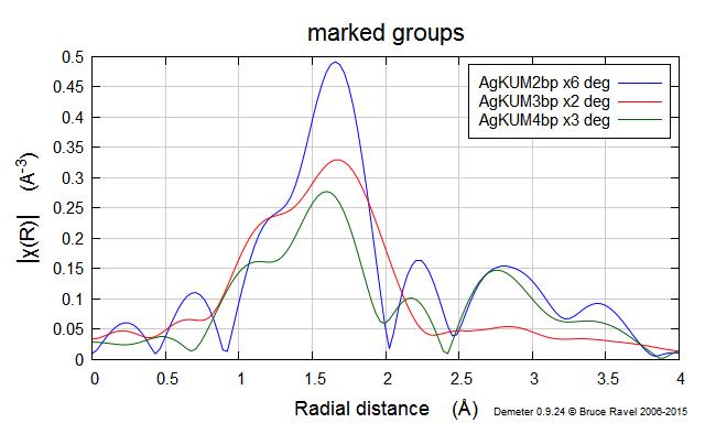 The goal of the visit was to discuss with Dr. Giuliana Aquilanti possibility of measurements on biologically active complexes at silver K-edge at XAFS beamline, which is under her supervision. Due to the fact that the energy of the K edge of Ag is close to the end of the beamline energy limit planning the experiment wasn’t trivial. After discussion and adjustment of the beamline settings the test measurements were performed on the Ag complexes of the coumarin derivatives. Since silver complexes are light sensitive, special sample preparation had been developed and used. The samples were measured in solid form and using transmission detection mode. Initial results indicated that all complexes in one measured series differs structurally. Data analysis will require a careful approach in order to find proper models which will describe investigated complexes. An example of the Fourier transformed EXAFS oscillations for the series of measured complexes is shown.
After successful test measurements a proposal for the upcoming call to the XAFS beamline at Elettra was decided to be prepared.
- • Dr. Jarosław Domagała – Task 2.2 - Visit to ESRF, Grenoble, France
In the framework of task 2.2 of work package "Enhancing of human potential through exchange of know-how and twinning activities with partnering organization" Dr. Jarosław Domagała visited ESRF, Grenoble, France, between July 4th – August 11th, 2016.
During the visit experimental results for rare-earth borate bulk crystals, which were considered for publication, have been discussed with Dr Jurgen Härtwig (BM05). In preparation is publication initially entitled “Growth and characterization of disordered rare-earth double borate laser hosts”.
During the visit two days of experiments were performed at BM05. A new diffractometer combined with a fast readout, low noise 2048*2048 Frelon camera coupled with a microscope optics which reduced the effective pixel size to 0.7μm, allowed to investigate in a very detailed way, with below arc second angular steps, the crystallographic perfection of the samples. The knowledge how to process the numerical data produced by camera was achieved. White beam topography images of volume GaN plates (results from 2015 visit at the ESRF) and new results for monochromatic beam were compared with data obtained by laboratory source equipped high resolution X-ray diffractometer (at IFPAN). An article about the defect structures of GaN platelets formed during crystal growth by HVPE characterized usingcomplementary laboratory and synchrotron sources will soon be submitted (initial title: ”Structural high-resolution x-ray characterization of the nonpolar substrate obtained by hydride vapor phase epitaxy”).
Further cooperation in the field of the characterization diamond samples for diamond based electronics (as well as for X-ray and gamma ray optics, what is a further program of interest) by high resolution X-ray diffraction (in Warsaw) was discussed with Dr. J. Morse from the ESRF – project leader of the application of diamond for detectors and diamond based power electronics, and with Dr. J. Härtwig together with Dr T.N. Tran Thi, who are the specialists in X-ray topography.
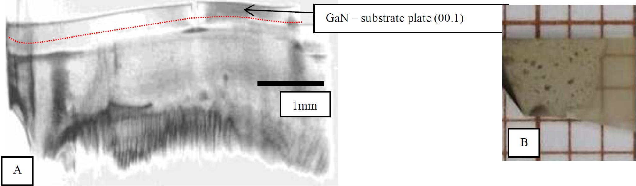
(A) White beam topograph. (B) Optical view of the sample with the etched part of the surface.
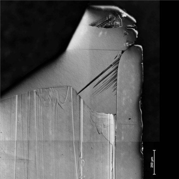
Monochromatic beam topograph. Optical view, area of interest with parasitic regrowth of the crystal.
As the result of the visitthe understanding of the defects appearing during the growth in volume GaN crystals obtained by HVPE technic with particular emphasis on edges parasitic areas has largely increased. An article about defect structures of GaN platelets formed during crystal growth by HVPE method will soon be submitted. A second article related to the study of the crystallographic quality of the rare-earth double borate was discussed with the “X-ray topography colleagues”. New cooperation in the field of diamond characterization was established. Newly acquired knowledge about the work with monochromatic wave topography – was implemented in practice.
- • Prof. Dr. hab. Maciej Sawicki – Task 2.8 - Visit to Institute of Semiconductors and Solid State Physics, Johanes Kepler University, Linz
In the framework of task 2.8 of work package "Enhancing of human potential through exchange of know-how and twinning activities with partnering organization" Prof. Dr. hab. Maciej Sawicki visited Institute of Semiconductors and Solid State Physics, Johanes Kepler University, Linz, between July 4th – 11th, 2016.
 To get familiar with the newest EpiTT in situ monitoring system which advances monitoring of the GaN-related structures growth for joint IFPAN-JKU investigations, to finalize a joint paper on the electric field modulation of the magnetic anisotropy in (Ga,Mn)N, and to establish directions of the future collaboration.
In-situ tools are used to observe in real-time the formation of the thin film throughout the thin film deposition process. LayTec’s EpiTT in-situ metrology system enables the development of new thin-film processes, materials and structures. In established processes, on the other hand, it is a must for high yields and maximum uptimes. 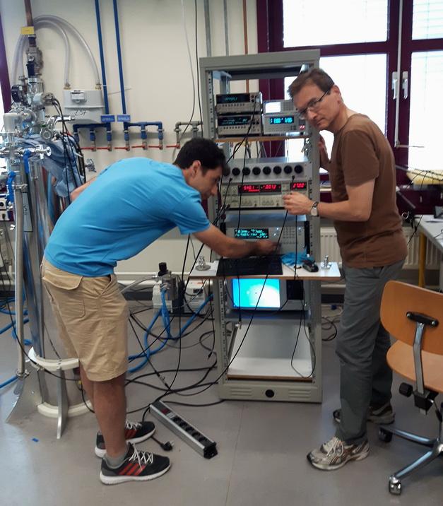 LayTec’s in-situ monitoring solutions are the most advanced on the market today and has recently been installed in the metal-organic vapor phase epitaxy system at JKU, and will be used to control the growth of layers structures to be investigated both at JKU and in IFPAN, at the Laboratory of Cryogenic and Spintronic Research. The EpiTT combines measurements of temperature and reflectance at three wavelengths in one tool. To establish the true temperature for materials that are transparent at 950 nm (GaN, Sapphire, SiC – which are of scientific interest to IFPAN scientists), EpiTT measures the temperature on the top side of the carrier. Measuring reflectance at three wavelengths monitors all essential properties of the growing layers, such as growth rate, film thickness, stoichiometry changes and morphology. New layers of GaN and (Ga,Mn)N structures have been grown during the visit. The first electrical tests of these layers have been performed with Dr. B. Faina.
The other part of the visit was devoted to finalize the recently prepared paper electric field modulation of the magnetic anisotropy in (Ga,Mn)N. The paper targets Nature Communication.
Finally, Prof. Sawicki discussed with Prof. A. Bonanni, the head of the NCore group at the Institute of Semiconductors and Solid State Physics, and Dr. R. Adhikari directions and specific targets of the future – post EAgLE – JKU – IFPAN collaboration. In particular, a joint project enabling mutual scientific contacts will be filed to the Austrian-Polish bilateral Program of Scientific and Technological Cooperation OEAD.
- • MSc. Marcin Stachowicz – Task 2.16 - Visit to HZDR (Dresden)
In the framework of task 2.16 of work package "Enhancing of human potential through exchange of know-how and twinning activities with partnering organization" MSc. Marcin Stachowicz visited HZDR (Dresden), between June 30th – July 15th, 2016.
The previous visits in HZDR allowed to get the first experience with new techniques of contactless measurements such as temperature dependent PL, PLE and EL, which shed light on the properties of materials of our interest. The PL and PLE spectra which were gathered during anterior twinning, have been the subject of study and basis of collaboration in the field of obtaining better structures without flaws present in the former series of zinc oxide layers implanted with rare earth ions.
 The epitaxial ZnO layers deposited by Atomic Layer Deposition (ALD) on a GaN/Al2O3 substrates were implanted at room temperature with 150 keV Yb3+ and Dy3+ ions to the fluency of 5x10¹⁴, 1x10¹⁵ and 5x10⁵ at./cm2. The channelling and Rutherford backscattering spectrometry demonstrated that initially above 97% of implanted rare ions occupy substitutional lattice positions. Subsequent annealing leads to partial recovery of the crystal lattice but also reduces substitutional fraction of RE ions. The temperature dependent PL and PLE studies conducted by Marcin Stachowicz, on as-implanted samples with below and above bandgap excitation revealed a very weak emission in the near-infrared region, which slightly increases with fluency of implantation in linear manner. The annealing process leads to the optical activation of ytterbium ions and significant improvement of the previously observed near IR emission. The optimisation of annealing temperature also gave gain to the emission intensity and the quality of crystallinity. The optimal temperature is 800oC, as results show, it leads to good recrystallization, when Zn is moved back to its substitutional site and rare earth ions are driven into interstitial sites. This conclusion is elaborated by taking under consideration of spectrometric and RBS/c results.
Noteworthy is that all samples were grown in the Institute of Physics Polish Academy of Sciences in Warsaw. The obtained electroluminescent spectra will be the subject of further detailed study and future publication and conference presentations (for instance at E-MRS Fall meeting 2016).
- • Dr. hab. Ewa Jędryka and Dr. hab. Marek Wójcik – Task 2.12 - Visit to ICMAB, Barcelona, Spain
In the framework of task 2.12 of work package "Enhancing of human potential through exchange of know-how and twinning activities with partnering organization" Dr. hab. Ewa Jędryka and Dr. hab. Marek Wójcik visited ICMAB, Barcelona, Spain, between June 30th – July 10th, 2016.
 During the visit at ICMAB regular meetings with prof. Fontcuberta and other members of his group were held. In particular, the possibilities to investigate modifications of properties of manganite thin films induced by application of electric field have been explored. The control of properties of magnetic oxides by application of electric field has been predicted theoretically. It opens a new and energetically more efficient way of controlling devices based on magnetic thin films. The use of NMR in such studies represents pioneering attempt in this respect. Two different systems of manganites are considered for this study. The first system is the optimally doped manganite films La2/3Sr1/3MnO3 deposited on ferroelectric substrate known in the literature as PMM_PT. The second studied system consists of films SrTiO3/La0.5Sr0.5MnO3. The ICMAB group reported recently that application of electric field crates polar areas around twinnings in SrTiO3 below phase transition temperature and this in turn influences mobility of domain walls and modifies the magnetic stiffness of manganite (La0.5Sr0.5MnO3). Possible variants of experimental conditions to be applied in the NMR experiments were analysed. In the course of the visit Dr. Wójcik presented the results of the joint study as an invited talk at the 12th International Workshop on Magnetism and Superconductivity at the Nanoscale, organized by the University of Barcelona.
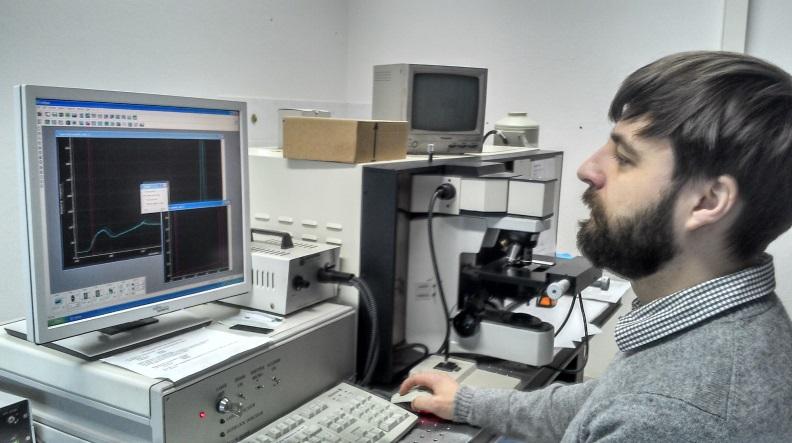
- • Dr. Roman Minikayev – Task 2.1 - Visit to Elettra Sincrotrone, Trieste, Italy
In the framework of task 2.1 of work package "Enhancing of human potential through exchange of know-how and twinning activities with partnering organization" Dr. Roman Minikayev visited Elettra Sincrotrone, Trieste, Italy between June 20th – 26th, 2016.
 During the visit, several meetings with Dr. Jasper Plaisier, the head of BL7.1 - MCX beamline at ELETTRA, took place. The meetings were devoted to analyzis and discussion of the results of "In-situ high temperature microstructure evolution of (Ga,Mn)As" – an ELETTRA scientific project. The data on the lattice parameter dependence of (Ga,Mn)As with temperature obtained within the project are shown in Fig. 1. The temperature range of the material stability and its thermal expansion within this range were determined.
Moreover the temperature of MnAs conglomerates formation in (Ga,Mn)As matrix during the annealing was verified. The crystallographic structure of MnAs precipitates was found. The lattice parameter and atomic positions were defined using the Rietved method.
- • Dr. Iraida Demchenko – Task 2.15 - Visit to Uppsala University, Sweden
In the framework of task 2.15 of work package "Enhancing of human potential through exchange of know-how and twinning activities with partnering organization" Dr. Iraida Demchenko visited Uppsala University, Sweden, between June 13th – 18th, 2016.
During the visit several laboratories, including XPS, among which a laboratory (equipped in HELIOS) stands out and is extremely promising in the field of time-resolved pump-probe spectroscopy research were visited. High Energy Laser Induced Overtone Source (HELIOS) an in-house laboratory for time-resolved pump-probe spectroscopy with extreme-ultraviolet (XUV) probe radiation. A wide span of pump wavelengths can be generated using commercial laser equipment while XUV probe radiation is generated via a high harmonic generation process in a noble gas delivering probe photons with energies between 20 and 72 eV. The XUV beam path features a time-preserving monochromator and was designed and constructed in-house. HELIOS features an overall time resolution of about 50 fs while using 800 nm pump and 41 eV probe photons. An energy resolution of 110 meV at 41 eV photon energy can be achieved. HELIOS features two beamlines. One μ-focus beamline with an XUV focal size of about 20 μm can be used for experiments that require such a small XUV focal size as well as with different end stations. The usability of the μ-focus beamline is demonstrated with time-resolved measurements on magnetic samples employing an in-house-designed spectrometer. These experiments allow the retrieval of element-specific information on the magnetization within a sample employing the transverse magneto-optical Kerr effect. The other beamline features a semi-permanently mounted end station for angle-resolved photoelectron spectroscopy under ultra-high vacuum (UHV) conditions. At the UHV beamline, the Angle-Resolved Time-of-Flight (ARTOF) spectrometer allow for a variety of different experiments. For instance, time-resolved photoelectron spectroscopy on solar cell related materials, aiming to investigate charge transfer in donor-acceptor interfaces could be done. The ARTOF allows for an investigation of the dynamics of correlated materials. Alternatively, the setup could be used, e.g., for measurements on organic molecules related to photo catalysis.
- • Dr. hab. Sławomir Kret – Task 2.3 - Visit to University of Warwick, Coventry, UK
In the framework of task 2.3 of work package "Enhancing of human potential through exchange of know-how and twinning activities with partnering organization" Dr. hab. Sławomir Kret visited niversity of Warwick, Coventry, UK, between April 13th – 26th, 2016.
The visit was focused on quantitative determination of the bismuth concentration in shells of GaAs/GaAlAS/GaBiAs nanowires grown by MBE method. Due to the fact that investigated nanowires have wurtzite structure, there is no data in literature concerning the limits of bizmuth incorporation in the wurtzite-GaAs. Successful quantification of the bismuth concentration in GaBiAs by EDS method will make a valuable contribution to understanding the properties of such bismuth-containing semiconductor compounds, which have a potential of being a new type of topological insulator nanostructures.
 Due to a relatively low concentration of bismuth in GaBiAs the quantification of elements' concentration required very good signal-to-noise ratio (S/N). Thanks to the electron probe correction system and extremely sensitive SSD-EDS detector installed on JEOL ARM microscope at the University of Warwick it was possible to achieve sufficient S/N ratio and quantify the distribution of bismuth in a very narrow shell. It was found that there is a 2nm-thick Bi-enriched subshell at the border of inner GaAlAs shell. High resolution data (not shown here) will be a part of a common paper concerning this kind of structures. The article will be submitted to high impact journal before the end of EAgLE project. Together with Richard Beanland a work on application of the digital scanning diffraction method (DSD) for studying local characteristics with nanometric resolution of mosaique in GaN/AlN heterostructures will be continued. Different algorithms suitable for high-precision automatic measurements of local rotations and lattice distortions will be tested. These algorithms rely on analysis of data stacks which may contain even several thousands of individual CBED patterns. The acquired data will be an object of future analysis. At the same time the development and improvement of algorithms for automatic analysis and creation of the ultrahigh resolution maps of local distortions of crystal lattice will be continued.
In summary, the visit gave the possibility to acquire new knowledge about quantification of minor elements' concentration with the use of new generation, large area SSD EDS detectors used in TEM microscope in STEM mode. Development and testing of new algorithms for high resolution strain mapping will allow to use the DSD method for studying the relaxation process in highly strained heterostructures of GaN/AlN.
- • MSc. Eng. Krzysztof Morawiec – Task 2.3 - Visit to University of Warwick, Coventry, UK
In the framework of task 2.3 of work package "Enhancing of human potential through exchange of know-how and twinning activities with partnering organization" MSc. Eng. Krzysztof Morawiec visited University of Warwick, Coventry, UK, between April 13th – 26th, 2016.
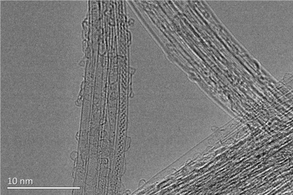
 During his visit Mr. Krzysztof Morawiec participated in investigation of carbon nanotubes filled with one dimensional crystals of two compounds: GeTe and Sb2Te3. The investigation was conducted on Jeol ARM 200F instrument which operates at the accelerating voltage of 200 kV and is equipped with a probe and image correctors. The aim of the investigation was to perform HRTEM imaging of single bundles of approximately parallel nanotubes (see Fig. 2). Previously the same samples were investigated at 300 kV, on Titan microscope at IFPAN, during the visit of dr Jeremy Sloan from University of Warwick. It turned out that due to the higher energy of the electron beam, the carbon nanotubes got damaged very quickly. It was expected that on the Jeol ARM instrument the degradation of crystal chains inside the nanotubes would not be as rapid. This turned out to be true, although the operator had to keep the exposure (electron dose) at very low level in order to minimize the damage. In these conditions it was possible to acquire low-dose focal series of high resolution images for future exit wave reconstruction (EWR) analysis.
 Additionally, diffraction patterns from bundles of filled nanotubes in a quantitative way were analysed. These patterns were obtained earlier using both Titan and Jeol instruments. The goal was to compare the specific features appearing around the central spot for different fillings of nanotubes. The experimental data will also be compared with diffraction patterns simulated for a modelled structure. In the future it is planned to investigate the effect of phase change of chains inside the nanotubes (from crystalline to amorphous) caused by heating. For this purposes diffraction patterns from samples which had undergone the phase change of crystalline fillings will be acquired and the whole process will be investigated in-situ.
As the result of the visit a new methods of investigation of phase transition in low dimensional composites by quantitative analysis of electron diffraction patterns has been developed.
- • Dr Grzegorz Łuka – Task 2.16 - Visit to HZDR Helmholtz Centrum Dresden Rossendorf Institute of Ion Beam Physics and Materials Research, Dresden, Germany
In the framework of task 2.16 of work package "Enhancing of human potential through exchange of know-how and twinning activities with partnering organization" Dr. Grzegorz Łuka visited HZDR, Dresden, Germany in April 13th – 20th, 2016.
During the visit dr. Luka worked in Dr. Wolfgang Skorupa group and he directly collaborated with Dr. Slawomir Prucnal. Dr Luka performed room temperature and temperature-dependent photoluminescence (PL) measurements of zinc oxide films co-doped with nitrogen and aluminium (ZnO:(N,Al)) as well as Yb-implanted ZnO films. ZnO(N,Al) films were deposited by atomic layer deposition (ALD) at IFPAN. The films were grown on c-sapphire substrates at two different growth temperatures (100 °C and 130 °C) and had two different thicknesses (~200 nm and ~1 µm). In total, four kinds of samples were investigated. Temperature-dependent PL spectra showed a PL band related to optical transitions involving defect states (related to N dopant) within the ZnO band gap.
ZnO films for the Yb implantation were deposited on GaN and Si single crystal substrates by the ALD method at IFPAN. Yb implantation and annealing were performed at HZDR. The samples were implanted by Yb ions with two different concentrations (five samples for each implantation). After implantation, two samples from each implantation process were additionally covered with a thin ZnO layer by the ALD. Then, the samples were annealed in N2 at two different temperatures, ~900 °C, and ~1000 °C (two samples, uncapped and capped one, were annealed in each process). As a result, 20 different samples were prepared for the PL measurements: 2 kinds of substrates × 2 different Yb concentrations × 5 samples for each implantation process. PL measurements were carried out at room temperature in visible (370 – 700 nm) as well as in the near infrared (IR) (800 – 1400 nm) spectral ranges. The spectra showed an inverse relation between near band gap and IR PL emission intensities, and these were conditioned by the sample treatment. The samples annealed at lower temperature (~900 °C) revealed lower band-gap emission and higher intensity IR emission compared to samples annealed at ~1000 °C. The IR emission, associated with transitions involving Yb states, was also higher for higher concentration ion implanted ZnO films.
During his stay, Dr. Luka performed RT and temperature-dependent PL measurements of the various kinds of ZnO and doped or implanted ZnO films. The measurements enable to indicate optimal growth and processing parameters of the investigated layers.
- • Dr. Anna Wolska, Dr. Marcin Klepka – Task 2.14 - Visit to Eu-XFEL, Hamburg, Germany
In the framework of task 2.14 of work package "Enhancing of human potential through exchange of know-how and twinning activities with partnering organization" Dr. Anna Wolska and Dr. Marcin Klepka visited Eu-XFEL, Hamburg, Germany in April 10th – 13th, 2016.
The visit was realized in answer to the invitation from Dr. Wojciech Gawelda. It was devoted to participation in a beamtime at Petra III synchrotron, beamline P01. The experiment concerned the time-resolved X-ray spectroscopy. This technique allows to follow the dynamics of the structural changes in samples under optical laser excitations. It can be very useful for studies of the photoinduced processes in biological samples. The aim of the experiment was to test possibility of studies on X-ray absorption of the nanoparticles of PEG coated ZnO diluted in the DMSO solution.
During that experiment we got acquainted with practical part of sample preparation, the adjusting of instrumentation and applied measurement’s techniques. This experiment tested whether possible applications of the time-resolved X-ray spectroscopy technique with the X-ray free electron lasers, like Eu-XFEL, can be used for this kind of materials.
- • Dr. hab. Marek Wójcik – Task 2.3 - Visit to Department of Physics, University of Warwick, Coventry, United Kingdom
In the framework of task 2.3 of work package "Enhancing of human potential through exchange of know-how and twinning activities with partnering organization" Dr. hab. Marek Wójcik visited Department of Physics, University of Warwick, Coventry, United Kingdom, between April 5th – 9th, 2016.
During visit M. Wojcik was hosted by prof. Geetha Balakrishnan from Superconductivity and Magnetism Group. Short visits have been organized in laboratories of several research groups at the Department of Physics such as Superconductivity and Magnetism Group, Surface, Interface & Thin Film Group and Microscopy Group, which gave an overview of experimental facilities and research interest. A special attention has been given to the research facilities and the scientific research of the Microscopy Group. Dr. Sanchez (a member of Microscopy Group) in collaboration with Dr. Beel (Surface, Interface & Thin Film Group) has initiated recently a program devoted to half-metallic materials at the atomic scale, which is closely related to the research interest of NMR group at IFPAN. During discussion it has turned out that scientists from Warwick and from Warsaw using different but complementary experimental techniques (TEM & STM and NMR) have been lead to very similar conclusions concerning properties of Co based Heusler compounds (e.g.Co2FeSi, Co2FeSi0.5Al0.5) which are considered as one of the most promising half metallic material for future spintronic applications. Both groups have found that either at the interface between the Si substrate and thin film of Heusler materials Co2FeSi0.5Al0.5 or in case of intentionally off- stoichiometric bulk materials such as Co2-xFeSi1+x and Co2Fe1-xSi1+x, (a) a strong preference for Si to substitute for Fe but not for Co, (b) a tendency of formation of Si rich CoSix compositions have been observed. These processes strongly modify the interface region between the Si substrate and CFSA and influence half metallic properties. This stimulated a discussion about possibilities to initiate a program of characterization of interface structures in magnetic oxides being of interest for the scientist from IFPAN using techniques available at the Microscopy Group in Warwick, namely advanced aberration corrected electron microscopy and spectroscopy.
- • Prof. Dr. hab. Grzegorz Karczewski – Task 2.6 - Visit to University of Wuerzburg, Experimentelle Physik III, Wuerzburg, Germany
In the framework of task 2.6 of work package "Enhancing of human potential through exchange of know-how and twinning activities with partnering organization" Prof. Grzegorz Karczewski visited University of Wuerzburg, between April 5th – 8th, 2016.
Semiconductor systems like PbSnTe with high Sn content and Bi2Se3 are new type of topological insulator material systems - topological crystalline insulators, in which the band structure is inverted and crystal symmetry (rather than time-reversal symmetry) determines the topology and protects the Dirac-like surface states. During his visit prof. Karczewski took part in a chain of meeting with prof. L. W. Mollenkamp and other members of the Experimentelle Physik III at Wuerzburg University devoted to set the final research plan on these and similar materials. It has been agreed that within the project prof. Karczwski will supervise (i) molecular beam epitaxy of high-quality relaxed CdZnTe layers on GaAs (and/or GaSb, InAs) and of PbSnTe layers on CdTe/GaAs buffers and directly on bulk CdZnTe substrates, (ii) characterization and optimization of the Pb(Sn)Te/CdTe interface with respect to low defect density and to low defect density and low intermixing, (iii) intentional doping of PbSnTe(Se) layer structures at the interfaces to CdTe, in the bulk, and in remote layers by dopants like Bi, Sb (iv) minimization of the bulk carrier density in PbSnTeSe by alloying with Se, and (v) studies of variation of lattice strain in PbSnTe layers by different Zn contents of the underlying relaxed CdZnTe buffer layers or CdZnTe substrates. A transfer of some of the characterization effort (MIR spectroscopy, SIMS and Rutherford backscattering) to IFPAN has been agreed.
- • Dr. Ryszard Sobierajski – Task 2.14 - Visit to European X-ray Free-Electron Laser Facility GmbH (Eu-XFEL)
In the framework of task 2.14 of work package "Enhancing of human potential through exchange of know-how and twinning activities with partnering organization" Dr. Sobierajski visited European X-ray Free-Electron Laser Facility GmbH, between April 5th – 8th, 2016.
The visit was devoted to the continuation of discussion about possible scientific collaboration. It evolved into formulation of a common research project that could be realized by means of the Femtosecond X-ray Experiments (FXE), at the European XFEL GmbH in Hamburg. The project is related to the studies of the crystal to amorphous phase transitions in metals.
I have also participated in preparation and realization of beamtime at Petra III synchrotron, beamline P01. The experiment was devoted to the time-resolved X-ray spectroscopy of biological samples. This experimental technique allows to follow the dynamics of the structural changes in samples under optical laser excitations. It can be very useful for studies of the photoinduced processes in biological samples. The aim of the experiment was to test and study X-ray emission, absorption and scattering channels. As a standard sample the Fe(CN)6 in water solution after pumping with optical laser was used. During that experiment I have learned about the technical difficulties common for the time-resolved X-ray spectroscopy technique with the X-ray free electron lasers, like Eu-XFEL.
- • MSc. Marcin Stachowicz – Task 2.16 - Visit to Helmholtz Zentrum Dresden Rossendorf, Semiconductor Materials Division
In the framework of task 2.14 of work package "Enhancing of human potential through exchange of know-how and twinning activities with partnering organization" MSc. Marcin Stachowicz visited Helmholtz Zentrum Dresden Rossendorf, Semiconductor Materials Division, between April 1st – 15th, 2016.
 This visit in the HZDR is a continuation of the previous one in March 2016. During this visit Marcin Stachowicz has continued the measurement of ALD ZnO samples doped with rare earth ions and annealed in different environments and techniques. Marcin Stachowicz has also started measurements of another types of samples which are ZnO based nanostructures, such as quantum wells and super lattices, and ZnO layers doped on p-type with such elements as nitrogen, antimony and arsenic. The p doped ZnO layers were grown on n-type substrates such as GaN templates. Although the PL and PLE measurements technique is the same as in the case of previous samples, the analysis approach is completely different, and another complementary measurement is required to characterise the samples properly, which is electroluminescence. The EL gave information about I-V characteristics in the DC bias mode under constant forward bias voltage and under different applied voltages in range of -2.4 up to 3.5 V. The calculated ideality factor is 1.8. The leakage current of 3x10-11 A for the reverse bias of -1V is observed. The results show that the investigated samples are potentially to be used as future UV photodetectors.
All investigated samples were grown in the Institute of Physics Polish Academy of Sciences in Warsaw. The obtained PLE temperature dependent and electroluminescent spectra will be the subject of further detailed study.
- • Prof. Dr. hab. Wojciech Szuszkiewicz – Task 2.10 - Visit to CEA – Saclay, Gif-sur-Yvette, France
In the framework of task 2.10 of work package "Enhancing of human potential through exchange of know-how and twinning activities with partnering organization" Prof. Dr. hab. Wojciech Szuszkiewicz visited CEA – Saclay, Gif-sur-Yvette, France, between March 28th – April 10th, 2016.
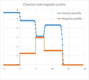 The visit was another great opportunity to continue the fruitful collaboration with French experts on neutron scattering techniques and to get familiar with different selected neutron spectrometers installed in this center. In particular, details and new experimental possibilities offered by the PRISM spectrometer installed on a cold neutron beam were introduced by Dr. Frederic Ott, a senior member of the lab and an expert in polarized neutron reflectivity. New, interesting and valuable results of PNR studies on Pt/Co/Pt trilayers irradiated by ultrashort laser pulses were obtained. The chemical and the magnetic profile of one from investigated trilayers, determined by the PNR is shown below. The ‘efficiency’ of nuclear and magnetic contribution to the total neutron scattering cross section as a function of a distance from the substrate surface (given in nm) is shown in this figure. The zero point corresponds to the substrate surface. It can be noticed that a partial alloying of Pt and Co layers took place, manifested by a presence of a magnetic signal outside of the area of the nominal Co layer in the middle of the structure. The results are an excellent proof of a high efficiency of the PNR experimental technique in the chemical and magnetic characterization of metallic nanostructures.
The newest experimental results from polarized neutron reflectivity research were accepted for presentations during the international conferences EMRS2016 hold in Lille (France) and JEMS2016 to be held in Glasgow in August this year. The manuscript of a paper reporting selected results of our joint studies has been sent to the JEMS Conference organizers and will be published as a contribution in the Journal of Physics Conference Series the next year.
- • Dr. Renata Ratajczak – Task 2.16 - Visit to HZDR Helmholtz Centrum Dresden Rossendorf
In the framework of task 2.16 of work package "Enhancing of human potential through exchange of know-how and twinning activities with partnering organization" Dr. Renata Ratajczak visited HZDR Helmholtz Centrum Dresden Rossendorf between March 9th – 24th, 2016.
The next visit at the Helmholtz Zentrum Dresden Rossendorf (HZDR) Dr. Renata Ratajczak and Dr. Sławomir Prucnal from HZDR started from a critical review of the previously obtained results of Raman, RBS/c and photoluminescence techniques on the ZnO implanted with Yb ions by both the traditional single step implantation and sequential double step implantations (in order to cumulate the fluency of 1×10¹⁵/cm2) and subsequently rapid thermal processing annealing (RTP), placing the main emphasis on further refinements of the experimental methodology and sample preparation. It was suggested that after further optimization measurements of PL and Raman spectroscopy will be continued on a new series of samples: epitaxial ZnO layers grown on GaN/Al2O3 substrate and on Si substrate, both implanted with Yb ions at 150 keV to fluence of 5×10¹⁴ at/cm2 and subsequently annealed by RTP for different annealing time at 800 ºC in O2 atmosphere.
The optical properties of implanted samples were studied by photoluminescence (PL) with a 355 nm from the UV laser excitation source with the power of 8 mW for two regions of interest: visible and infrared (IR). In IR region PL from Yb was observed. The excitation mechanism itself is well known. Because the excitation energy is higher than the ZnO band gap the RE ions are excited indirectly. Optically injected electrons and holes form excitons in the ZnO film which lead to excitation of the 4f shell of Yb ions. A very weak PL from the sample after implantation to fluence of 5×10¹⁴ at/cm2 have been observed. In case of implanted and annealed samples some spectral lines at the wavelengths of 980, 1027, 1047 and 1072 nm have been observed. The most prominent peaks lying at 980 nm, correspond to the main transition energies from the excited 2F5/2 to the 2F7/2 ground state of Yb3+. Broad peaks situated between 1000-1100 nm correspond to the Yb3+ ion emission vibronic band and the PL intensity is about 2 times higher for ZnO/GaN than for ZnO/Si. In the visible region PL coming from ZnO band gap and defects was observed. In case of ZnO/Si very intensive green and red PL coming from defects have been observed. The obtained PL spectra will be the subject of further detailed studies.
- • MSc. Marcin Stachowicz – Task 2.16 - Visit to HZDR (Dresden)
In the framework of task 2.16 of work package "Enhancing of human potential through exchange of know-how and twinning activities with partnering organization" MSc. Marcin Stachowicz visited HZDR (Dresden), between March 9th – 24th, 2016.
 The results of PL and PLE measurements conducted during first visit in HZDR were the basis of further experimental work at IFPAN. Part of the samples have been thermally annealed in different environments and using different techniques and new ones have been obtained. This imposed the need of conducting the same measurements on temperature modified samples and using another contactless and non-destructive technique which is Raman spectroscopy.
As the PL and PLE spectra of as implanted ZnO: Yb and Er spectra were of low intensity and fast subsiding with temperature, the emission intensity of annealed samples was much higher. Depending on environment, time and technique of annealing, even an order of magnitude more intensive was the emission from the sample. The spectra lines became more confined which allows for deeper analysis of the character of emission. The Raman spectroscopy measurement conducted at room temperature allows to investigate the change of the crystallinity as the method is very sensitive to small changes in material structure. The results obtained with Raman spectroscopy requires an experience in analysing the spectra, in which the first group of samples were ALD ZnO: Er and Yb of different thickness grown on c-plane Al2O3 substrates. Second set of samples was similar to the previous one but grown on Si substrates. All samples were grown in the Institute of Physics Polish Academy of Sciences in Warsaw. The obtained PLE temperature dependent and RT Raman spectra will be the subject of further detailed study.
- • MSc. Łukasz Owczarczyk – Task 2.13 - Visit to DUT, Dortmund, Germany
In the framework of task 2.13 of work package "Enhancing of human potential through exchange of know-how and twinning activities with partnering organization" MSc. Łukasz Owczarczyk visited DUT, Dortmund, Germany between March 6th – 16th, 2016.
 During the visit in Dortmund Technical University at the group headed by prof. Manfred Bayer a training in advanced spectroscopic techniques was obtained. The main topic was the use of Mono-Vista confocal micro Raman/micro PL spectrometer for polarization-dependent spatial-resolved PL spectroscopy of Quantum Dots(QD) II-VI compounds based nanostructures. During this training spatial-resolved spectra of CdSe/ZnSe QD (manufactured in SL.3 laboratory of IFPAN) in different excitation condition were investigated and processes of energy transfer between excitons in ZnSe barrier excitons in CdSe QD have been studied.
Also, a training in a use of pico- and femtoseconds tuneable lasers (Ti-Sappfire Coherent inc. “Mirra system) and OPO (“Faros-Orfeus-Lira” system from Light Conversion ltd.) yook place.
Finaly, a short training in using time-resolved Kerr rotation (TRKR) spectrometer was carried out.
- • Dr. Vitalii Ivanov – Task 2.13 - Visit to Dortmund Technical University
In the framework of task 2.13 of work package "Enhancing of human potential through exchange of know-how and twinning activities with partnering organization" Dr. Vitalii Ivanov visited Dortmund Technical University, between February 21st – April 30th, 2016.
During of the stay in Dortmund Technical University (DTU) in the group of prof. Manfred Bayer (21.02.205 – 30.04.2016) a following tusks have been realized:
– Training in operation of wide band tuneable (in the range 400 nm – 2400 nm) femto- and pico second laser system based on optical parametric oscillator (OPO).
– Training in application of spin-noise technique to ODMR spectroscopy of DMS nanostructures.
– Training in application of two-colour ultrafast spectroscopy of Faraday and Kerr rotation (with using of ultrafast OPO system).
– Experimental study of spin dynamic of 2DEG in modulated doped CdMnTe/CdMgTe DMS QW and NV-centers in diamond crystals
by time-resolved ODMR and ultrafast two-colour magneto-spectroscopy.
– Preparatio to submission the article “Resonantly enhanced spin-lattice relaxation of Mn2+ ions in diluted magnetic semiconductors (Zn,Mn)Se/(Zn,Be)Se quantum wells”.
 We studied an optical properties of 2DEG with high mobility in modulated doped (MD) CdMnTe/CdMgTe and CdTe/CdMgTe QW nanostructures (which have been manufactured in IFPAN) with a help a time-resolved and polarization resolved magneto-optical and microwave spectroscopy. In optical probing Quantum Hall regime a strong polarization of 2 DEG by high frequency microwave excitation (60GHz) has been observed. Phonon less non-resonant excitation of strongly correlated electron system by microwave quanta has been detected at the first time. Also a first experimental observation of spin bistability of electron system in CdMnTe/CdMgTe DMS MD QW has been realized using pulse-probe time-resolved magneto-optical spectroscopy techniques.
Study of spin-kinetic in an ensemble of NV- - centers in diamond crystals also gave a new results, which could find an applications in technology. Firstly, at room temperature ultra-low strength of electromagnetic field (less than 2.5 μA/m!) has been detected at regime of ODMR in NV- - centers micro ensemble. This effect is due to very long spin relaxation times of NV- - centers excited states which are uncoupled with environment. Secondly, we have observed optically excited W-band (60 GHz) microwave amplification in NV-centers enriched diamond crystals tunable by magnetic field due to saturation of spin transitions of isolated nitrogen impurity ground state.
 Finally, at this visit our joint project devoted to study of mechanism of spin relaxation in a system of isolated Mn2+-ions spins and spin clusters of Mn2+ was finalized: an article of J. Debus, V.Yu.Ivanov, S.M.Ryabchenko et al.. "Resonantly enhanced spin-lattice relaxation of Mn2+ ions in diluted magnetic (Zn,Mn)Se/(Zn,Be)Se quantum wells" has been finalized and submitted to PRB. In this paper, we performed the results of first direct observation of resonant phonon less energy transfer from isolated Mn2+ ions to different types of Mn2+ clusters (Fig. 1).
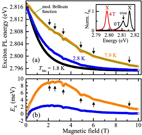
FIG. 1. (a) Giant Zeeman shift of the exciton PL energy for sample no. 2 measured at different CW excitation powers 6mW/cm2 (TMn = 1.8 K), 0.7 W/cm2 (2.8 K), and 8.8 W/cm2 (7.9 K); T = 1.8 K. The cusp positions are marked by arrows. Inset: normalized PL spectra for B = 0 and 4 T; P = 0.7W/cm2. (b) Difference of the exciton energies, EX(TMn) − EX(1.8 K), for P = 0.7 and 8.8 W/cm2 shown by blue and orange, respectively.
- • Dr. Anna Wolska, Dr. Marcin Klepka, Dr. Ryszard Sobierajski, Dr. Anna Reszka, and Dr. Dorota Klinger-Teuchmann – Task 2.14 - Visit to European X-ray Free Electron Laser Facility
In the framework of task 2.14 of work package "Enhancing of human potential through exchange of know-how and twinning activities with partnering organization" Dr. Anna Wolska, Dr. Marcin Klepka, Dr. Ryszard Sobierajski, Dr. Anna Reszka, and Dr. Dorota Klinger-Teuchmann visited European X-ray Free Electron Laser Facility, between January 27th – 29th, 2016.
The participation in the Eu-XFEL users’ meeting and its satellite workshops offered a perfect opportunity to become familiar with the recent developments and current status of the European XFEL, advances in the instrument design as well as selected science applications. The special attention was focused on the time resolved studies of the structural dynamics by means of x-ray techniques like x-ray absorption and emission spectroscopy, x-ray scattering, photon correlation spectroscopy. A great deal of usefull details about the recent activities and plans for the FXE and MID instruments were given. The first instrument aims at the time-resolved investigation of ultrafast processes in condensed-matter systems. Scientific areas of application are chemical dynamics, dynamics of condensed matter and matter under extreme conditions. The second one aims at the investigation of nanosized structures and nanoscale dynamics using coherent radiation. Especialy usefull were presentations by Dr. Klaus Soklowski-Tinten about the irreversible material dynamics studied by single-pulse time-resolved X-ray scattering and by Dr. Peter Zalden about crystallization dynamics of phase-change materials resolved by ultrafast x-ray. Basing upon these lectures possible common research activities with leading XFEL scientists were discussed. Other lectures presented with recent advances in the theory of the intense x-ray pulses interaction with matter. Especialy important were those given by Dr. Baerbel Rethfeld about ultrafast laser-induced magnetization dynamics in metals and by Dr. Nikita Medvedev about nonequilibrium, nonthermal and nonadiabatic effects in FEL-excited semiconductors. During the discussion which followed the lectures potential theoretical approaches to the modelling of the experimental data obtained were established.
As the result of the visit an extended knowledge about the time-resolved structural characterization of matter (in particular spectroscopic tracking the chemical reactions, spectroscopy on solids and interfaces. X-ray scattering on nanoparticles) by means of X-ray free electron lasers like Eu-XFEL has been gained. Furthermore, common research activities were defined with leading XFEL scientist, in particular regarding the theoretical modelling of experimental data and future research project at Eu-XFEL.
- • MSc. Michał Grzybowski – Task 2.11 - Visit to The University of Nottingham, Physics and Astronomy Faculty
In the framework of task 2.11 of work package "Enhancing of human potential through exchange of know-how and twinning activities with partnering organization" MSc. Michał Grzybowski visited The University of Nottingham, Physics and Astronomy Faculty (Group of Spintronics and Ferromagnetic Semiconductors), between January 10th – March 22nd, 2016.
The research allowed the visitor to get expertise in fabrication of CuMnAs based devices grown on GaP substrate. A study of the photolithography process and possible photolithography defects with its influence on the electrical signals was performed. The anisotropic magnetoresistance (AMR) effect on different CuMnAs devices was studied. Comparison of the temperature and substrate influence on the current-induced switching was conducted.
Familiarisation with simultaneous application of electrical (AMR) and photoemission electron microscopy (PEEM) was also important part of the visit. Together, the applied techniques allow observation of the domain pattern of the material, identification of pronounced changes of the domains under the influence of current-induced torques, and determination of the dependence on current magnitude.
This research revealed a sub-micron scale magnetic domain structure (Fig. 1) which is modified by successive current pulses applied along orthogonal axes. At this stage, learning of image processing and attempts to perform quantitative analysis of PEEM images was important. It led to a demonstration of clear correlation between domain images and electrical signals recorded as part of the same pulse sequence (Fig. 2).

Fig. 1 The PEEM image of CuMnAs surface Fig. 2 Electrical signals measured for CuMnAs switching.
with domain structure visible.
Measurements were performed using the facilities disposed by University of Nottingham and Diamond Light Source (UK) with the supervision and tight cooperation with members of Group of Spintronics and Ferromagnetic Semiconductors (UoN). Studies described above and many discussions led to the observation of domain changes in PEEM and its consistency with electrical signals. Performed research is promising in terms of application some of these experimental protocols in other antiferromagnetic materials in the future in IFPAN.
- • MSc. Roger Kalvig – Task 2.2 - Visit to European Synchrotron Radiation Facility in Grenoble, France
In the framework of task 2.2 of work package "Enhancing of human potential through exchange of know-how and twinning activities with partnering organization" MSc. Roger Kalvig visited European Synchrotron Radiation Facility in Grenoble, France, between October 11th – December 19th, 2015 and January 3rd – 23rd, 2016.
During the internship a series of XAS Mn K - edge experiments on Mn5Ge3Cx (x=0, x=20%, x=40%, x=50%, x=85%) thin films (30 nm thick) have been prepared and performed on Bending Magnet 23 at room temperature. The aim of this study was to determine crystal structure, investigate the quality of Mn5Ge3 thin films grown on different substrates (Ge(111) and GaAs(111)), compare the properties of samples grown by two different growth methods (Solid Phase Epitaxy and Reactive Deposition Epitaxy) and investigate the effect of carbon doping in Mn5Ge3Cx films. Raw experimental data have been treated with the Athena software. Subsequently data modelling has been carried out by Artemis software within Demeter package created by Bruce Ravel. Based on literature data, a model has been created to fit single shell of absorbing atoms and it was found that films grown on GaAs(111) substrate reveal much lower quality, disordered structure than those prepared on Ge(111) substrates. Moreover, investigation of carbon – doped Mn5Ge3 films grown by SPE technique indicated that some distances from absorber to nearest neighbours are slightly longer than in case of films grown by RDE method. Analysis of carbon - doped films grown on Ge(111) by SPE is not very clear. A preliminary conclusion is that carbon may substitute Mn atoms in Mn5Ge3Cx lattice. Results obtained for highly doped Mn5Ge3C0.85 indicate that MnC clusters are probably more easily created in Mn5Ge3 lattice than filling subsequent interstitial sites by carbon atoms if carbon concentration exceeds 50%.
- • Prof. Dr. hab. Maciej Sawicki – Task 2.16 - Visit to HZDR Helmholtz Centrum Dresden Rossendorf Institute of Ion Beam Physics and Materials Research, Dresden, Germany
In the framework of task 2.16 of work package "Enhancing of human potential through exchange of know-how and twinning activities with partnering organization" Prof. Dr. hab. Maciej Sawicki visited HZDR, Dresden, Germany, between December 14th – 22th, 2015.
During the visit at the HZDR Helmholtz Centrum Prof. Sawicki took part in a series of meetings led by the head of the Institute Prof. Manfred Helm and Dr. Shengqiang Zhou. The main theme of these discussions was an elaboration of the present stage of the joint collaborative effort in research of magnetoelectrical and magnetic properties of III-V dilute magnetic semiconductors (GaAs, In As, and GaP) with a sizable contents of transition metals (Mn or Fe) introduced by means of ion beam implantation and ultra-fast laser-assisted re-growth technique. This method allows for manufacturing single phase dilute magnetic semiconductors with transition metal contents exceeding frequently that of molecular beam epitaxy growth technique. Also, the different preparation method offers unique abilities to test correctness of some theoretical prediction which connect the certain properties of these materials, like the magnetic anisotropy, with some mechanism taking place during the growth. During the meetings the already obtained results of both groups were compared, analysed, and the prospects for forthcoming publications were set.
As a part of the visit, on Thursday, 17th Dec 2015, Professor Sawicki delivered a talk entitled: “Magnetic order at the localization boundary”, a subject being at the core of the interest of both groups in these studies. After the seminar, a vivid discussion has led to an elaboration of new experimental techniques more suitable for magnetometric studies of magnetic semiconductor layers at the localisation boundary.
- • Dr. Renata Ratajczak – Task 2.16 - Visit to HZDR Helmholtz Centrum Dresden Rossendorf
In the framework of task 2.16 of work package "Enhancing of human potential through exchange of know-how and twinning activities with partnering organization" Dr. Renata Ratajczak visited HZDR Helmholtz Centrum Dresden Rossendorf between December 7th – 16th, 2015.
The visit began with the review of the results obtained during the previous visit, in October 2015. Dr. Renata Ratajczak and Dr. Sławomir Prucnal from HZDR discussed results of Raman, RBS/c and photoluminescence (PL) techniques obtained for ZnO implanted with Yb ions and subsequently annealed using different techniques: Furnace Tube (FA), Rapid Thermal Procces Annealing (RTP) and Flash Lamp Annealing (FLA).
Upon the conclusions from the discussions a study of an optimization of the of ZnO implantation with RE commenced, using the same techniques as previously: Raman spectrometry, RBS/c and PL. The structural and optical analysis were performed for two series of implanted samples:
1. Single step traditional Yb ion implantation (dose: 1×10¹⁵ at/cm2 at 150 keV) and annealing (RTP for 20 min at 800 ºC in O2)
2. Sequential double-step Yb ion implantation (does: 5×10¹⁴ at/cm2 at 150 keV) and annealing (RTP for 10 min at 800 ºC in O2) after each step.
The Raman spectroscopy measurements were performed under guidance and supervision of Dr. Słąwomir Pruncal using a 532 nm Nd:YAG laser. It was found that subsequent annealing reduced the intensity modes of ZnO and increased those of Yb. It proves that annealing partially recovers the crystal lattice structure and also substantially reduces amount of substitutional fraction of Yb atoms. For sequential double-step Yb ion implantations the Raman spectrum do not reveal any differences.
Further information were inferred from RBS/c measurements. In both cases also an out-diffusion of Yb atoms process is observed. The optical properties of implanted samples were studied by photoluminescence (PL) with a 355 nm from the UV laser excitation source. The most prominent peak lies at 980 nm and corresponds to the main transition energies from the excited 2F5/2 to the 2F7/2 ground state of Yb3+. Broad peaks situated between 1000-1100 nm correspond to the Yb3+ ion emission vibronic band.
Sequential double-step Yb ion implantation (5×10¹⁴ at/cm2 at 150 keV) and annealing (RTP for 10 min at 800 ºC in O2) after each step revealed better structural recovery and higher photoluminescence of Yb3+ in comparison to the samples implanted in a single step (1×10¹⁵ at/cm2 at 150 keV) and annealed once by RTP (20min at 800 ºC in O2). The obtained PL and RBS/c as well as Raman spectra will be the subject of further detailed studies by HZDR – IFPAN team.
- • Prof. Dr. hab. Elżbieta Guziewicz – Task 2.16 - Visit to HZDR Helmholtz Centrum Dresden Rossendorf
In the framework of task 2.16 of work package "Enhancing of human potential through exchange of know-how and twinning activities with partnering organization" Prof. Elżbieta Guziewicz visited HZDR Helmholtz Centrum Dresden Rossendorf between December 7th – 10th, 2015.
During the visit at the HZDR Helmholtz Centrum Prof. Guziewicz discussed with Prof. Wolfgang Skorupa and Dr. Sławomir Prucnal the recent experimental results on zinc oxide films grown in the Atomic Layer Deposition laboratory. Prof. Guziewicz also gave a talk entitled: „Electrical and optical properties of semiconducting and dielectric films grown by Atomic Layer Deposition technique”. A series of ZnO samples implanted with Yb ions were also measured by Raman spectroscopy with a 532 nm Nd:YAG laser. The ZnO:Yb samples annealed at different conditions (sequential multiple implantation-annealing processes and traditional annealing) have been compared. The results are presented in Fig. 1 and Tab.1. Interpretation of the obtained Raman spectra is difficult because of multiple active modes originating from ZnO, GaN i Al2O3 materials. The most significant changes are observed for Raman modes 167, 535 i 574 cm-1. The former one derives probably from RE and is a fingerprint of substitutional incorporation of RE in ZnO. The decreased intensity of 574 cm-1 mode (A1(LO)) show a recovery of ZnO structure as a result of annealing.
- • Prof. Dr. hab. Wojciech Szuszkiewicz – Task 2.10 - Visit to Commissariat à l'énergie atomique (CEA)
Centre de Saclay, France
In the framework of task 2.10 of work package "Enhancing of human potential through exchange of know-how and twinning activities with partnering organization" Prof. Wojciech Szuszkiewicz visited Commissariat à l'énergie atomique (CEA) Centre de Saclay between December 6th – 14th, 2015.
During my stay in the Nuclear Research Center (CEA) in Saclay (France) I had an opportunity to visit laboratory dealing with neutron beams and to discuss selected experimental details related to investigations of structure and magnetic properties of magnetic thin layers and multilayers with the use of polarized neutron reflectivity (PNR). Dr. Frederic Ott, the senior scientist in this laboratory and an expert in polarized neutron reflectivity has shown me and explained in details experimental possibilities offered by new modifications of the PRISM spectrometer, installed on a cold neutron beam with the neutron wavelength equal to 0.42 nm. With the use of this spectrometer one can check an influence of the external magnetic field on magnetic properties of sample under investigation. It is possible to apply magnetic fields up to 2 T and to perform the reflectivity measurements as a function of temperature from about 10 K to the room temperature. Dr. Ott has shown me also the results of his last experimental investigations with the use of neutrons and explained me his recent achievements in the area of semiconductor and metal physics.
The visit to offered also an excellent opportunity to perform the PNR test measurements. I have taken advantage of metallic magnetic multilayers on the basis of Co and Pt, grown at the Institute of Physics PAS by the MBE technique. Such multilayers are of interest due to their possible applications in the area of information storage and are intensively investigated at numerous research centers. The results of our PNR measurements completed presently available results of other studies like, e.g., XRD, EXAFS and MOKE, which have been performed on the same multilayers the last year by the research team from the Institute of Physics PAS and from the University of Białystok. Our first common paper entitled “Polarized neutron reflectivity and X-ray scattering measurements as tools to study properties of Pt/Co/Pt ultrathin layers irradiated by femtosecond laser pulses” has been recently accepted for publication in the “Phase Transitions” journal.
- • MSc. Dmitr Snigurenko – Task 2.6 - Visit to HZDR (Dresden)
In the framework of task 2.16 of work package "Enhancing of human potential through exchange of know-how and twinning activities with partnering organization" MSc. Dmitr Snigurenko visited HZDR (Dresden) between November 26th – December 3rd, 2015.
During the visit at the HZDR Helmholtz Zentrum I gathered experience in Photoluminescence measurements of undoped ZnO films and ZnO films doped with nitrogen (ZnO:N) after FLA annealing at different voltages and in various atmospheres. The results were compared with the previous results on ZnO and ZnO:N film which were annealed by rapid thermal processing (RTP) in O2 and N2 atmosphere at 500ºC during 3 minutes.
ZnO thin films were grown at the Institute of Physics PAS by the ALD method at different deposition temperatures (100 -200ºC). After the growth the samples were treated by a short time annealing (20 ms) by Flash Lamp (FLA) in O2 atmosphere using different voltages (3.6 kV and 3.8 kV). Hall effect measurements of ZnO and ZnO:N samples after different type of annealing were performed. As a result of FLA annealing concentration of free carriers decreases by one order of magnitude in case of the samples deposited at 200°C, but we do not observe any change of the conductivity type. In the ZnO films without intentional doping (S2058, B556) we observe shifting of absorption lines towards lower energy after FLA annealing.
FLA annealing in a nitrogen atmosphere of the ZnO:N films result in a significant change of the intensity of defect-related photoluminescence measured at room temperature (Fig. 2). Unfortunately we cannot compare PL after FLA annealing in nitrogen and oxygen atmosphere, because samples annealed in O2 atmosphere do not reveal any PL signal.
Fig 2. PL RT for ZnO:N before and after FLA annealing.
- • Prof. Dr. hab. Maciej Sawicki – Task 2.8 - Visit to Johannes Kepler University Linz, Austria
In the framework of task 2.8 of work package "Enhancing of human potential through exchange of know-how and twinning activities with partnering organization" Prof. M. Sawicki visited Johannes Kepler University, Linz, Austria between November 26th – December 3rd, 2015.
 It was mainly a collaborative meeting with group of prof. Alberta Bonanni of JKU Linz to discuss the recently obtained results on gated (Ga,Mn)N-containing structures, methods of their growth, and to set the next directions of the collaborative effort in magnetotransport measurements of Linz’s grown spintronics materials at IFPAN. To this end two group meetings were hold at which Prof. Sawicki (from IFPAN side) and Dr. R. Adhikari and Dr. A.T. Martin-Luego (from JKU side) presented the results and discussed the challenges lying ahead. The main emphasis was put forward on the recently obtained results of the magnetic studies in SQUID based magnetometer performed on gated-at-IFPAN structures which were grown in Linz. To facilitate further studies new structure layouts were discussed over and the decision were made about the directions to move ahead.
The other part of the visit was devoted elaboration of techniques and best methods for low temperature studies of other (Ga,Mn)N contating structures, namely those suiitable for investigations of spin current generation in so called spin-filter arhitecture and spin pumping affects. To this end some relevant samples were tested in a new magnetortansport station and Prof. Sawicki took part in the experimental elaboration of the best low temparature experimental conditions. This tast was performed with Drs R. Adhikari and B. Faina.
As the results of the visit further direction for JKU-Linz – IFPAN collaboration in gating experiments of (Ga,Mn)N containing structures were established and conditions for low temperature studies at IFPAN of samples with spin-filter architecture were elaborated.
- • Dr. Grzegorz Łuka – Task 2.16 - Visit to HZDR Helmholtz Centrum Dresden Rossendorf Institute of Ion Beam Physics and Materials Research, Dresden, Germany
In the framework of task 2.16 of work package "Enhancing of human potential through exchange of know-how and twinning activities with partnering organization" Dr. Grzegorz Łukai visited HZDR, Dresden, Germany between November 26th – December 1st, 2015.
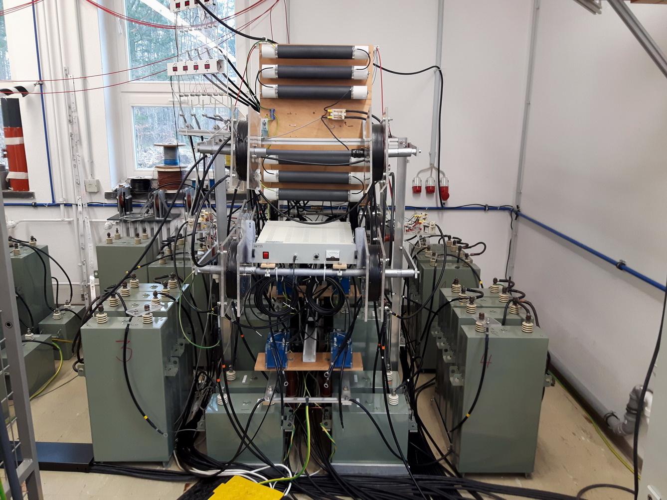 The aim of the visit was to acquire knowledge on ion implantation of II-VI compounds by transition metal elements.
During the visit at the HZDR Helmholtz Centrum dr. Luka discussed with Dr. Shengqiang Zhou and Dr. Slawomir Prucnal the details of the training and work planned for 2016 in HZDR. The planned collaboration will include ion implantation of wide band gap semiconductor thin films by transition metals, flash lamp annealing of the as grown doped or ion-implanted samples, and optical measurements.
Additionally, the basics of flash lamp annealing technique have been acquired. This technique enables very fast (~ several tens of milliseconds) heating the surface of the sample and subsequent equally fast recrystallization of the molten layer. In that way, the sample recrystallization with negligible ion diffusion is possible.
Fig. The capacitor bank of the flash lamp annealing set-up.
- • MSc. Marcin Stachowicz – Task 2.16 - Visit to Helmholtz Zentrum Dresden Rossendorf, Semiconductor Materials Division
In the framework of task 2.16 of work package "Enhancing of human potential through exchange of know-how and twinning activities with partnering organization"MSc. Marcin Stachowicz visited Helmholtz Zentrum Dresden Rossendorf, Semiconductor Materials Division, between November 17th and December 16th, 2015.
ZnO has received considerable attention as a candidate material for optoelectronic devices such as blue light-emitting and short-wavelength laser diodes with low thresholds in the UV region. Its unique property of a large exciton binding energy (60 meV) leads to the existence and extreme stability of excitons at room temperature (RT) and even higher temperatures, which makes ZnO a highly efficient photon emitter.
The temperature dependent Photoluminescence (PL) and Photoluminescence excitation (PLE) measurements of the Zinc Oxide materials was the aim of the visit in the Helmholtz Zentrum in Dresden. First group of samples were thin layers of ZnO grown on sapphire substrates and nitrogen doped during the growth process by Molecular Beam Epitaxy (MBE). Second type of samples were Zno/ZnMgO quantum structures embedded into nanocolumns deposited on Si substrates by MBE. Third group were quantum structures of ZnO/ZnMgO double asymmetric quantum wells grown on sapphire substrates obtained by MBE. And finally fourth group of samples were ZnO layers grown on GaN templates by Atomic Layer Deposition (ALD) and implanted with rare earth, such as Yb and Er. All samples were grown in the Institute of Physics Polish Academy of Sciences in Warsaw. The obtained PL and PLE temperature dependent spectra will be the subject of further detailed study.
- • MSc. Pavlo Konstantynov – Task 2.4 - Visit to Visit to ALBA Synchrotron Facility (Spain)
In the framework of task 2.4 of work package "Enhancing of human potential through exchange of know-how and twinning activities with partnering organization" MSc. Pavlo Konstantynov visited Visit to ALBA Synchrotron Facility (Spain) between November 14th, 2015 – March 1st, 2016.
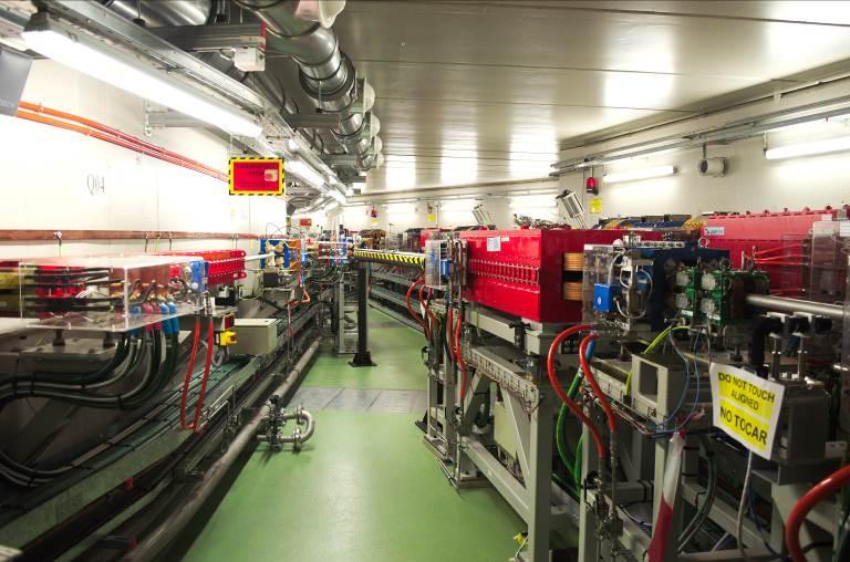 During the first week of my visit, November 16-20, 2015, I participated in the workshop entitled “WIEN2k and Turbomole” co-organized by IF PAN group of "X-ray spectroscopy and microanalysis" specialists, namely, Dr. Y. Melikhov, Dr. P. Rejmak, Mr. Y. Syryanyy, and Dr. hab. I.N. Demchenko. The workshop was split into two parts devoted to WIEN2k and Turbomole numerical codes, respectively. Each section consisted of 3 lectures (explanation of the scientific method in general, introduction into a specific numerical code, and advanced usage of the numerical code), followed by the hands-on experience, during which the participants were taught how to solve various examples.
 The rest of my visit was devoted fully to my research area of interest, which lies in the field of x-ray spectroscopy, through participation in the discussions with the beamline scientists of BOREAS, CIRCE and CLAESS beamlines. During these discussions I was improving existent or getting a basic knowledge about experimental techniques exploited at these beamlines. Majority of the time of my visit at ALBA was devoted to acquaintance with the X-ray Magnetic Circular Dichroism (XMCD) spectroscopy technique at BOREAS beamline. In addition to participation in such type of experiments and in addition to fruitful discussions of the results, I developed and wrote the processing code for XMCD data analysis using Python programming language under scientific guidance of dr Eric Pellegrin. The applicability of my program was verified on the XMCD data for Co, Ni and Fe. Another fruitful cooperation with dr Pellegrin and Mr Harold Moreno was related to the project currently run at ALBA synchrotron facility aiming to design a system to clean by plasma etching optical elements of various shapes and dimensions used at ALBA. The effectiveness of the plasma cleaning process is currently being tested on EUV mirrors at ALBA synchrotron facility. Such technique could lead even to the ability to clean the whole chambers at the beamlines.
Finally, thanks to several guided tours, which were performed by dr A. Nosych, I was seen the sections of the synchrotron facility which are often hidden from ordinary users including linear accelerator (linac) and several transfer points where beam is passed from the storage ring to beamlines. These tours allowed me to expand my knowledge about the beam formation, orbit control and adjustment, different types of beam diagnostics systems etc.
- • Dr. Iraida Demchenko, Dr. Yevgen Melikhov, Dr. Pawel Rejmak, MSc. Yevgen Syryanyy – Task 2.4 - Visit to ALBA Synchrotron Facility (Spain)
In the framework of task 2.4 of work package "Enhancing of human potential through exchange of know-how and twinning activities with partnering organization" a group of SL1.2 researchers visited ALBA Synchrotron Facility starting from November 14th 2015: Dr. Iraida Demchenko (two months visit), Dr. Yevgen Melikhov (one month visit), Dr. Pawel Rejmak (one month visit) and MSc. Yevgen Syryanyy (two weeks visit).
The first week of the scientific visit was devoted to the running of the workshop organized by our group titled “WIEN2k and Turbomole Workshop” (November 16-20, 2015). The workshop was split into two sections: WIEN2k (leading person Dr. Melikhov) and Turbomole (leading person Dr. Rejmak) numerical codes. Each section consisted of 3 lectures (explanation of the scientific method in general, introduction into a specific numerical code, and advanced usage of the numerical code), followed by the hands-on experience, during which the participants solved various examples.
Since the research area of interest of IP PAS scientists lies in the field of x-ray spectroscopy, we used the scientific visit as an opportunity to familiarize ourselves with the beamlines and endstations which are closely related to our research area of interest: BOREAS (Resonant Absorption and Scattering), CIRCE (Photoemission Spectroscopy and Microscopy) and CLAESS (Core Level Absorption & Emission Spectroscopies) beamlines. Fruitful discussions with the beamline scientists and with Dr. Eric Pellegrin, Supervisor of soft x-ray beamlines - Physics section, were conducted during which the issues related to the mentioned beamlines were highlighted.
For example, we were able to familiarize ourselves with the unique possibility to perform XPS measurements at near ambient pressure at CIRCE beamline (NAPP endstation), where measurements at pressures up to 20 mbar can now be conducted allowing investigations of surfaces in situ under more realistic environments real-world conditions (i.e. in the presence of gases and, possibly, liquids), such as in the case of interfacial chemical reactions in catalysis, chemical vapor deposition, electrochemistry and environmental chemistry. As another example, Dr. Demchenko studied in details the experimental techniques and data analysis approach to soft-XAS (including XMCD) and XPS data used at BOREAS beamline. More specifically, the training in CTM4XAS55 software, a software for analysis of transition metal L-edge XAS (including XMCD), Electron Energy Loss Spectroscopy (EELS), and XPS was conducted by Dr Pellegrin, which allowed to process the results of the XPS measurements realized at “Surface Science Lab” at IP PAS. Among other fruitful discussions, we would like to highlight several which could lead or led already to joint projects and publications: Dr. Demchenko, Dr. Melikhov and Mr. Syryanyy discussed with Prof. M. Aranda (Scientific Director), Dr. L. Simonelli (Beamline CLAESS Responsible Officer), O. Matilla (Head of Electronics Section) and Dr. E. Pellegrin (EAgLE coordinator at ALBA) a successful submission of the joint grant application “Novel detector based on GEM technology for synchrotron x-ray spectroscopy applications” submitted to FET-Open call of Horizon-2020 program (H2020-FETOPEN-2014-2015-RIA call) on September 29, 2015; Dr. Rejmak discussed with Prof. Aranda the applicability of periodic DFT calculations to study the selected properties of pure and doped calcium aluminates, being the component of new, fast-binding cements; Dr. Demchenko and Dr. Melikhov discussed with Dr. Simonelli, Dr. C. Marini (Beamline Scientist) and Dr. W. Olszewski (Post-Doctoral Research Associate) the manuscript under preparation devoted to the XAFS measurements performed on CLAESS beamline on GaMnAs thin films; Dr Rejmak met with Dr. Ibraheem Yousef (from MIRAS beamline) to discuss issues of combining experimental and computational techniques in infrared (IR) spectroscopy.
- • Dr. Aleksandra Drzewiecka-Antonik – Task 2.1 - Visit to Elettra, Sincrotrone Trieste
In the framework of task 2.1 of work package "Enhancing of human potential through exchange of know-how and twinning activities with partnering organization" Dr. Aleksandra Drzewiecka-Antonik visited the Elettra synchrotron, located close to Trieste, Italy in the period of November 13th - November 19th, 2015.
This visit was devoted to the measurements at XAFS beamline within ongoing cooperation between part of the group of the X-ray spectroscopy and microanalysis at IP PAS and XAFS group at Elettra. Throughout the whole duration of this research visit, I felt tremendous support from the beamline researchers – Dr. Luca Olivi and Dr. Giuliana Aquilanti.
Selected copper complexes with coumarin derivatives were investigated. Measurements were performed at Cu K-edge for both powdered and liquid samples. For the microcrystalline complexes the transmission detection mode was used whereas for liquid samples the fluorescence detection mode was required. In the case of liquid samples – dimethyl sulfoxide and dimethylformamide were used as solvents.
Initial results indicated that the solvent molecule can be incorporated into the complex structure causing the modification of the metal coordination sphere. This can be linked with biological properties of studied compounds which will be the subject of our further consideration.
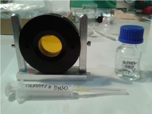
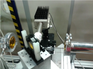
Overall, the project led to a deeper understanding of XAFS measurements of the liquid samples. The undertaken structural study of Cu complexes with coumarin acids and its derivatives will help in understanding the mechanism of the metal-ligand binding which is important since these compounds possess biological activity.
- • Prof. Ewa Jędryka, and Prof. Marek Wójcik – Task 2.12 - Visit to the Institut de Ciència de Materials de Barcelona (ICMAB-CSIC) , Bellaterra, Spain
In the framework of task 2.12 of work package "Enhancing of human potential through exchange of know-how and twinning activities with partnering organization" Prof. Ewa Jędryka and Prof. Marek Wójcik visited the EAgLE scientific partner, Prof. J. Fontcuberta a head of the research group “Multifunctional Oxides and Complex Structures” in the Institut de Ciència de Materials de Barcelona (ICMAB-CSIC), Bellaterra, Spain, in the period: November 4th – November 8th, 2015.
The aim of this short visit was twofold. The first task was to prepare a final version of the paper titled : “Strain-driven orbital and magnetic orders and phase separation in epitaxial half-doped manganite films” reporting the results of investigations of strain effect on structural and magnetic properties of thin films of half – doped manganites La0.5Sr0.5MnO3. These materials have recently attracted renewed attention because their ground state can be modified by engineering the bandwidth or by modifying their carrier density. This property makes them ideal materials for integration in reconfigurable ferroelectric tunnel junction (FTJ) with potentially large tunnel electro-resistance effect (TER). The paper reports the results obtained by linear/circular polarized x-ray absorption and by 55Mn NMR to explore the role of structural distortions and electronic bandwidth on the orbital occupancy and spin ordering of Mn-3d states in La0.5Sr0.5MnO3 films under various strain states.
A second purpose of the visit was to discuss a new interpretation of the observed effect of strain on the hypefine field experienced by nuclei of Mn ions located in tetragonally distorted oxygen octahedral of perovskite structure. A possibility of using NMR to detect an orbital polarization of Mn 3d (eg) state of such ions caused by strain has been formulated by the team from IFPAN. It was suggested that strain generated at the interface between ferroelectric layer and manganite layer biased by external electric field could be an excellent experimental verification of the above effect. ICMAB group declared to prepare a special sample for such 55Mn NMR experiment.
- • Dr. Roman Minikayev and Prof. Dr. hab. Wojciech Szuszkiewicz – Task 2.2 - Visit to European Synchrotron Radiation Facility (ESRF) Grenoble, France
In the framework of task 2.2 of work package "Enhancing of human potential through exchange of know-how and twinning activities with partnering organization"Dr. Roman Minikayev and Prof. Dr. hab. Wojciech Szuszkiewicz visited European Synchrotron Radiation Facility (ESRF) Grenoble, France in the period of October 6th - October 14th, 2015.
During our stay in the European Synchrotron Radiation Facility (ESRF) in Grenoble (France) we had an opportunity to visit the biggest and the most modern laboratory dealing with synchrotron radiation. We have discussed selected experimental details related to investigations of structure and dynamic properties of various solids including both bulk crystals and low-dimensional structures like, e.g., thin layers and multilayers.
We had also a possibility to perform the test measurements related to lattice dynamics of bulk lead chalcogenides – materials attracting recently a lot of attention because of their particular properties. First of all, these semiconductors exhibit excellent thermoelectric properties and find a variety of applications. Secondly, some of them are known as ‘crystal topological insulators’ and determination of the properties of such insulators is one of very hot topics today in the area of solid state physics.
We had a pleasure to collaborate with Dr. Alexei Bosak, an excellent scientist and a member of ESRF staff. Dr. Bosak is responsible for ID28 beamline, where a spectrometer dedicated for measurements of inelastic X-ray scattering on excitations in solids is installed. With the use of this spectrometer one can investigate not only phonons, but also other excitations present in crystals. A few different synchrotron radiation wavelength are available with the use of ID28, it is also possible to check an influence of temperature and an external magnetic field on the sample properties. With the use of synchrotron radiation energy of 17794 eV and the spectral resolution of 3 meV we have tested two samples at room temperature: pure PbTe crystal and the solid solution (Pb,Cd)Te containing 2% of CdTe. The lattice dynamics has been determined along a few high-symmetry directions in the Brillouin zone. The obtained results are in a perfect agreement with the results of our previous inelastic neutron scattering studies and will be a topic of future common publication. Dr. Bosak explained us also in detail the experimental opportunities with the use of ID28 beamline.
- • Dr. Renata Ratajczak and MSc. Dmitr Snigurenko – Task 2.16 - Visit to HZDR Helmholtz Centrum Dresden Rossendorf
In the framework of task 2.16 of work package "Enhancing of human potential through exchange of know-how and twinning activities with partnering organization" Dr. Renata Ratajczak and MSc. Dmitr Snigurenko visited HZDR Helmholtz Centrum Dresden Rossendorf between October 4th – November 7th, 2015.
During the visit at the Helmholtz Zentrum Dresden Rossendorf the basics of the joint collaboration on ZnO implantation with Rare Earth (RE) elements has been established. The visitors completed a training course familiarizing them with the techniques of the optical studies: Raman spectroscopy and photoluminescence (PL). Training also included full course on service of the experimental set-up and data acquisition systems. The course was carried out by Dr. Slawomir Prucnal from HZDR, who also assisted and supervised the subsequent optical measurements performed during the rest of the visit.
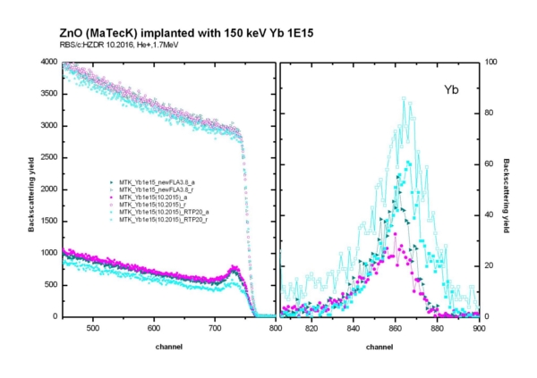 Two types of ZnO crystals were investigated: single crystals and ALD layers grown on GaN/Al2O3. The samples were implanted in Warsaw with Yb ions with different fluences: 5×10¹⁴, 1×10¹⁵, and 2×10¹⁵ at/cm2. Ion implantation is a very convenient technique for introducing RE ions into a crystal lattice, because impurity concentration and its depth profile can be easily controlled. Unfortunately, the ballistic nature of the implantation process, leading to the damage of crystal lattice, reduces the light emission efficiency. In order to cause the structure recovery heat treatment usually is applied. However, annealing process causes also to RE-ions relocation and optical activation of dopant atoms. Therefore, the investigations of the structural and optical changes induced by implantation of Yb-ions combined with subsequently annealing (with different thermal conditions) on ZnO are highly important.
For quick FLA annealing process the out diffusion of Yb on the crystal surface was not observed. During the FLA annealing the RE atoms move to substitutional positions. The substitutional fraction is better than after RTP annealing, but the Yb3+ peak in the near-infrared region is very weak. This suggests that during the implantation followed by FLA annealing Yb ions are in the 2+ valence state. Figure shows RBS/c spectra obtained for ZnO implanted with 1×10¹⁵ at/cm2 Yb ions and annealed using RTP as well as FLA.
- • Dr. Marcin T. Klepka, Dr. hab. Eng. Anna Wolska, Dr. Eng. Ryszard Sobierajski, Dr. Aleksandra Drzewiecka-Antonik – Task 2.1 - Visit to Elettra, Sincrotrone Trieste
In the framework of task 2.1 of work package "Enhancing of human potential through exchange of know-how and twinning activities with partnering organization" Dr. Marcin T. Klepka, Dr. Anna Wolska, Dr. Ryszard Sobierajski and Dr. Aleksandra Drzewiecka-Antonik visited the Elettra synchrotron, located close to Trieste, Italy in the period of September 28th - October 9th, 2015.
The goal of the first part of the visit was to perform Grazing Incidence X-Ray Fluorescence (GI-XRF) and grazing incidence X-Ray Reflectometry (XRR) experiments at XRF beamline at Elettra synchrotron. The measurements were performed on the Pt/Co/Pt thin layers fabricated at the IP PAS. Different types of samples were investigated: as-grown (with an in-plane magnetisation) and irradiated by intense extreme UV nanosecond and optical femtosecond pulses (with out-of-plane magnetisation). The purpose of the study was to correlate the observed magnetic changes with structural ones. The detailed analysis and understanding of the data is one of the topics of further collaboration. During the visit we got acquainted with the upgraded XRF beamline instrumentation and control system. We also learned about possible applications of the GI-XRF technique to study the structure of the thin layers.
Second part of visit was devoted to the measurements at XAFS beamline within ongoing cooperation between part of the group of the X-ray spectroscopy and microanalysis at IP PAS and XAFS group at Elettra. Head of the XAFS group is Dr. Giuliana Aquilanti.
Selected copper complexes with thiourea derivatives (these with significant inhibition against S. aureus, S. epidermidis, B. subtilis, B. cereus and M. luteus) were investigated. Measurements were performed at Cu K-edge (8979eV) for powdered and liquid samples. For the microcrystalline complexes the transmission detection mode was used whereas for liquid samples (which concentration was in the mmol range) the fluorescence detection mode was required. In the case of liquid samples – dimethyl sulfoxide (DMSO) and dimethylformamide (DMF) were used as solvents. Initial results indicated that the solvent molecule can be incorporated into the complex structure causing the modification of the metal coordination sphere. This can be linked with biological properties of studied compounds which will be the subject of further consideration.
- • Dr. Iraida Demchenko, Dr. Yevgen Melikhov, MSc. Pavlo Konstantynov, and Prof. Dr hab. Elżbieta Guziewicz – Task 2.1 - Visit to Elettra Sincrotrone, Trieste, Italy
In the framework of task 2.1 of work package "Enhancing of human potential through exchange of know-how and twinning activities with partnering organization"Dr. Iraida Demchenko, Dr. Yevgen Melikhov, MSc. Pavlo Konstantynov, and Prof. Dr hab. Elżbieta Guziewicz visited the Elettra synchrotron, located close to Trieste, Italy in the period of September 27th - October 9th, 2015.
The scientific goal of the research visit to the ELETTRA synchrotron, Material Science Beamline (6.1L), was to increase academic qualifications in the field of resonant photoemission through the realization of research project #20150152-ELETTRA entitled "Zinc oxide films implanted with Rare Earth for optoelectronic applications".
Within the proposal #20150152-ELETTRA, resonant photoemission (ResPES) experiment was used to investigate the ytterbium electronic states and their hybridization with valence electrons of zinc oxide. Both commercial single ZnO crystals (obtained from Mateck company) and epitaxial ZnO films grown by Atomic Layer Deposition (ALD) technique were under investigations. The ZnO thin films were grown in the IP PAS (prof. E. Guziewicz group). Ytterbium ions were incorporated into the ZnO matrix via implantation (at the level of 1015 and 1016 cm-2) and subsequent annealing (for different times). For successive realization of the photoemission experiments, Ar+ sputtering and annealing of the investigated samples up to ~573 K were performed. Photoemission spectra were taken across the RE4d – RE4f photoionization threshold. The Fermi level was determined by measuring a response from Mo holder which was in electrical contact with the sample.
We found that for ZnO implanted by Yb there is a very little resonant enhancement of the valence band. Such observation is consistent with a large 4f14-δ occupancy. Moreover, it was found that ytterbium 4d level for investigated samples shows extended multiple structure instead of simple spin-orbit doublet for metallic ytterbium. Such observation allowed us to conclude that majority of ytterbium atoms are bonded to oxygen and show an extended multiple structure indicating that one of the 4f14 electrons has been promoted to the valence level. This multiple structure can be attributed to 4fn → 4d9 interaction. Subsequent theoretical investigations are necessary to confirm our work hypothesis.
Throughout the whole duration of this research visit, we felt tremendous support from all Materials Science Beamline researchers: our especial gratitude belongs to prof. Kevin Prince, Beamline Coordinator, dr Martin Vondráček, Beamline Scientist, and dr Stanislav Cichoň, PostDoctoral Research Associate, who were able to pass their knowledge in an interesting, friendly and professional manner.
Overall, the project led to a deeper understanding of ResPES measurements including not only ability to follow the procedure and to perform experiments but also to perform a focused data analysis. All of that adds significant value for increase of research potential at the IP PAS.
- • Dr hab. Ewa Jędryka and Dr. hab. Marek Wójcik – Task 2.7 - Visit to NCSR 'Demokritos' Institute of Nanoscience and Nanotechnology, Athens
In the framework of task 2.7 of work package "Enhancing of human potential through exchange of know-how and twinning activities with partnering organization" Dr hab. Ewa Jędryka and Dr. hab. Marek Wójcik visited NCSR 'Demokritos' Institute of Nanoscience and Nanotechnology, Athensin the period of September 25th - October 2nd, 2015.
NCSR "Demokritos" is the largest multidisciplinary research centre of Greece, specializing in the fields of Nanotechnology, Energy & Environment, Biosciences, Particle and Nuclear Science, Informatics and Telecommunications. The NMR group of IF PAN collaborated intensively with the 'Demokritos' researchers in the years 1995-2000, carrying out two joint NATO research projects. The results of these projects have been published in two Phys. Rev. B papers and a number of conference presentations. Present visit in the Institute of Nanoscience and Nanotechnology of Demokritos Centre was concentrated on talks with prof. Kalliopi Trohidou and prof. Evangelos Hristoforou. It was decided to prepare a joint project with prof. Hristoforou concerned with elaboration of sensors applicable in drug delivery. NMR experiment in Warsaw would be used to characterize the nanoparticles prepared in Athens with the aim of transporting a pharmaceutical compound in the body in order to achieve a desired therapeutic effect.
The latest results of the NMR group in Warsaw, applicable to the use in magnetic sensors have been presented during the IC-MAST meeting organized by Prof. Evangelos Hristoforou.
- • Dr. Marcin T. Klepka, Dr. hab. Eng. Anna Wolska – Task 2.14 – Visit to European X-ray Free-Electron Laser GmbH
In the framework of task 2.14 of the work package "Enhancing of human potential through exchange of know-how and twinning activities with partnering organization" Dr. Marcin Klepka and Dr. Anna Wolska from IF PAN visited the European X-ray Free Electron Laser (Eu-XFEL) facility in the period of August 12th - 17th, 2015.
The visit was realized in answer to the invitation from Dr. Wojciech Gawelda. It was devoted to the continuation of discussion about possible future scientific collaboration. The main goal was to find joint field to be studied using Femtosecond X-ray Experiments (FXE), at the European XFEL GmbH in Hamburg.

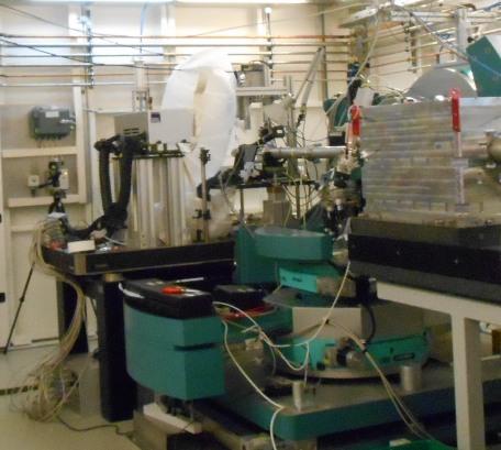

We have also participated in preparation and realization of beamtime at Petra III synchrotron, beamline P01. The experiment was devoted to the time-resolved X-ray spectroscopy of biological samples. This experimental technique allows to follow the dynamics of the structural changes in samples under optical laser excitations. It can be very useful for studies of the photoinduced processes in biological samples. The aim of the experiment was to test and study X-ray emission, absorption and scattering channels. As a standard sample the Fe(CN)6 in water solution after pumping with optical laser was used.
- • Dr. Vitalii Ivanov – Task 2.13 – Visit to Dortmund Technical University
In the framework of task 2.13 of the work package "Enhancing of human potential through exchange of know-how and twinning activities with partnering organization" Dr. Vitalii Ivanov visited Dortmund Technical University in the period of August 1st - 15th, 2015.
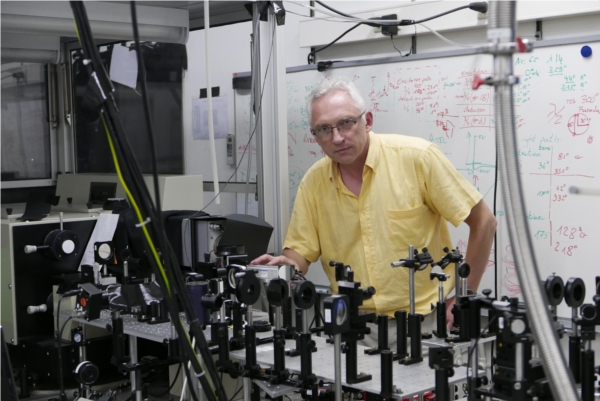 During of the stay in Dortmund Technical University (DTU) in the group of prof. Manfred Bayer (01.08.2015-15.08.2015) a following tasks have been realized:training in the application of polarization resolved magneto-spectroscopy of techniques to investigation on energy transfer mechanisms in diluted magnetic semiconductors nanostructures -quantum dots (QD) and quantum wells (QD) has been carried out;
characterization of novel semiconductors nanostructures (ZnMnTe/ZnMgTe QW) (manufactured in IFPAN) using time-resolved magneto PLE spectroscopy has been done.
Results of the experiments has been discussed with Prof. M. Bayer, Prof. D. Yakovlev and Prof. E.Zhukov from DTU. Article “Spin-relaxation and enenergy transfer in II-VI DMS nanostructures(Zn,Mn)Te/(Zn,Mg)Te DMS quantum wells” has been performed.
- • MSc. Michał Grzybowski – Task 2.11 – Visit to The University of Nottingham, Physics and Astronomy Faculty
In the framework of task 2.11 of the work package "Enhancing of human potential through exchange of know-how and twinning activities with partnering organization" Mr. Michał Grzybowski visited The University of Nottingham, Physics and Astronomy Faculty (Group of Spintronics and Ferromagnetic Semiconductors) in the period of July 21st - August 22nd, 2015.
 Fig.1 The example of electron transport measurements of CuMnAs showing the longitudinal resistance vs temperature. Three colour curves are for different configurations of in-plane magnetic field applied.
The research plan of the visit was focused on learning AMR (anisotropic magnetoresistance) techniques of antiferromagnetic thin films of CuMnAs and devices fabrication based upon this material. The particular features of performed research activity are good control of high temperatures and high thermal stability demands. Since CuMnAs is an antiferromagnetic material with the Néel temperature around 430 K, phenomena related to the critical behaviour can be observed in that region of temperatures. The main feature observed is the extremum of derivative of resistivity of temperature. This is a footprint of Néel temperature which varies among the samples and its full width at half maximum can give information about the magnetic homogeneity of the sample.
The next step included learning the techniques of studying the AMR effect in fixed temperature of high stability (long stabilisation times and experiments conducted in dedicated copper chamber with halogen lamp) and varying magnetic field value and angle in antiferromagnetic based CuMnAs hall bar devices. The measurements revealed the strong temperature dependence of resistivity while no significant and systematic influence of magnetic field up to 0.4 T was observed.
 Fig.2 The example of the part of AMR measurements in varying magnetic field and stable temperature. No influence of magnetic field is observed here and significant changes of resistivity reflect well the temperature fluctuations.
Measurements were performed using the facilities disposed by University of Nottingham with the supervision and tight cooperation with members of Group of Spintronics and Ferromagnetic Semiconductors (UoN). Studies described above and many discussions led to the conclusions that the magnetic susceptibility of studied samples has no influence on AMR effect in studied range of magnetic field and temperature values. Temperature fluctuations had the major role of resistivity changes of studied thin films. Performed research is promising in terms of application of these experimental protocols in other antiferromagnetic materials or other ranges of temperatures or magnetic field values.
- • Dr. hab. Sławomir Kret – Task 2.3 - Visit to Department of Physics, University of Warwick, United Kingdom
In the framework of task 2.3 of work package "Enhancing of human potential through exchange of know-how and twinning activities with partnering organization"Dr. hab. Sławomir Kret on 5 July to 18 July 2015 visited the EAgLE scientific partner Department of Physics, University of Warwick, United Kingdom.
During visit together with Dr. Richard Beanland and Dr. Ana Sanchez we tested the ability of the Scanning Digital Electron Diffraction (SDED) method to study the local strain and relative crystal lattice rotations of segments in core shell nanowires. The method, which was developed initially in electron microscopy group of University of Warwick, is based on acquisition of the series of diffraction patterns for each position of the subnanometric electron beam during scanning of analysed area. For example, for 30 x 60 nm area 1800 individual diffraction patterns were acquired as digital images on CCD camera (beam step Δx, Δy = 1 nm). Each individual diffraction pattern contains information about electron scattering properties of the column of diameter of 1-2 nm (depending on the convergence angle of the beam, diameter and thickness of investigated material). By analyzing such patterns it is possible to determine the local rotation of crystalline lattice with mil-radian precision and to determine the components of the strain tensor by measuring distances between Bragg spots. In the case of a complex structure like GaAs/InGaAs/AlGaAs core shell nanowire this method will permit to obtain the 2D maps of strain components and understand the strain state evolution as the function of the composition and thickness of the core and the shells of NWs. Nevertheless independent information about local elemental composition is needed. We have also tested simultaneous acquisition of elemental composition with the same spatial resolution from the same analysed volume of material as in the case of SEDD by using EDS and EELS spectroscopy. In the case of implementation of this method at IFPAN we plan to develop software which will perform automatic analysis of diffraction patterns “on fly” and reduce the amount of data (hundreds of gigabytes).
- • Dr. Maciej Zgirski – Task 2.9 – Visit to Aalto University, Espoo, Finland
In the framework of task 2.9 of the work package "Enhancing of human potential through exchange of know-how and twinning activities with partnering organization" Dr. Maciej Zgirski visited Aalto University, Espoo, Finland in the period of July 5th - 11th, 2015.
During the visit measurements of the sample at miliKelvin temperatures were performed. We could measure temperature relaxation of small metallic nanoislands subject to intentional heating. We investigated heat flow between two such nanoislands. The measurement concentrated also on getting familiar with cross-correlation technique based on frequency multiplexing. The acquired results will be used for upcoming common publication.
A great deal of knowledge about heat transfer in nanostructures at miliKelvin temperatures was gained. This involves:
• familiarizing with mechanisms of energy exchange (temperature relaxation) in nanostructures (electron-phonon coupling,
hot electron diffusion, relaxation through emission of photons),
• calorimetry of nanoobjects,
• familiarizing with state-of-the-art experiments in heat transfer of on-chip circuits.
This part of acquired expertise lends strong support to the on-going experiments at Laboratory of Cryogenic and Spintronic Research in IFPAN aimed at measurements of temperature relaxation in superconducting and normal wires with Josephson junction probed with the current pulses. In future I am planning to perform on-chip calorimetry with Josephson junction in cooperation with the twinning partner.
- • Prof. Ewa Jędryka, and Prof. Marek Wójcik – Task 2.12 - Visit to the Institut de Ciència de Materials de Barcelona (ICMAB-CSIC) , Bellaterra, Spain
In the framework of task 2.12 of work package "Enhancing of human potential through exchange of know-how and twinning activities with partnering organization"Prof. Ewa Jędryka and Prof. Marek Wójcik visited the EAgLE scientific partner, Prof. J. Fontcuberta a head of the research group “Multifunctional Oxides and Complex Structures” in the Institut de Ciència de Materials de Barcelona (ICMAB-CSIC), Bellaterra, Spain, in the period: July 2nd – July 14th, 2015.
The aim of the visit was to discuss the results of new NMR experiments carried out at IFPAN on two groups of manganite thin films grown in ICMAB and to plan further NMR experiments on these systems: (a) half doped manganites tetragonaly distorted by strain exerted due lattice mismatch to substrates, (b) optimally doped manganite films capped by different diamagnetic oxides creating additional interface.
 The results of NMR experiments on half doped manganites provided a microscopic picture of ferromagnetic DE phase reduction and transformation of the metallic conductivity to weekly conducting state. Moreover, the in-field NMR data provided strong arguments supporting the new interpretation of the 55Mn NMR spectrum for moderately strained LSMO5/STO. The NMR line is regarded as representative for Mn ions remaining in a mixed valence state but with the hole preferentially moving within 3d eg(x2-y2) orbitals, which is a precursor to A type antiferromagnetic state observed in bulk materials for x>0.5 as a ground state. These joint results have been presented during the conference ICM as a poster titled : Strain induced phase separation in thin films of half-doped La0.5Sr0.5MnO3 manganites: 55Mn NMR studies.
A draft of the paper reporting both 55Mn NMR and linear/circular polarized x-ray absorption data tilted - Strain-driven orbital and magnetic orders and phase separation in epitaxial half-doped manganite films has been discussed.
The second topic discussed was the problem of deterioration of magnetic and conducting properties of optimally doped manganite La2/3Sr1/3MnO3 (LSMO) being in contact with another oxide of perovskite structure. In this project 55Mn NMR experiment was used as a probe of charge distribution and of Mn spin state in LSMO ultra-thin films. The aim was to explore the effect of strain and bonding at the interface between manganite and ABO3 capping layer. It was found that capping with LAO and STO (to less extend) brings back the degeneracy of Mn eg(3d) orbitals and recovers the DE phase, whereas in case of SZO, the asymmetry of the Mn eg(3d) orbitals is strengthened, leading to expansion of the AF phase. These joint results have been presented during ICM as the poster titled: Overlayer-induced reconstruction of Mn orbitals in manganite thin films studied by 55Mn NMR and are being prepared for a publication as a joint paper with the ICMAB group.
- • Prof. Dr. hab. Maciej Sawicki – Task 2.12 – Visit to Institut de Ciencia de Materials de Barcelona, Catalunya, Spain
In the framework of task 2.12 of the work package "Enhancing of human potential through exchange of know-how and twinning activities with partnering organization" Prof. Maciej Sawicki visited visited Institut de Ciencia de Materials de Barcelona, Catalunya, Spain between July 2nd – 11th, 2015.
The aim of the visit was to discuss the details of the ultra-high sensitivity magnetic and microwave measurements in strip-line configuration and to present the latest stage of the development of the understanding and functionalization of a new insulating ferromagnetic compound (Ga,Mn)N to a broader international audience during the 20th International Conference of Magnetism which took place in Barcelona during the visit.
 During the visit at ICMAB regular meetings with Prof. Sanchez and other members of the Multifunctional Oxides and Complex Structures group have been carried out. Main emphasis was put on discussing experimental techniques and tricks employed by the group to gain normally not attainable sensitivity in magnetic SQUID and in strip-line microwave measurements.
The main outcome of the discussions on magnetometry was the realisation of a tiny, but previously uncounted, contribution from the long extension of the sample holder. It was pointed out that this contribution can affect results of magnetic studies of samples composed of a minute magnetic layer deposited on a bulky substrate. Test measurements were performed. Analysing their results some ideas how to mitigate this problem were put forward and they will be checked and possibly implemented in home lab of Prof. Sawicki at the IFPAN.
During the lab tour the main attention was put on the role and the method of usage of micromanipulators for precise microwave measurements in strip-line configuration. Prof. Sawicki spent considerable amount of his time at ICMAB on learning the best techniques of using such a device and how to take out the best of it during microwave measurements.
During the stay in Barcelona Prof. M. Sawicki also presented results of studies which led to the elaboration of the origin of ferromagnetic order in (Ga,Mn)N – a new insulating ferromagnetic compound. The presentation was an invited lecture during the 20th International Conference of Magnetism, an event which gathered more than 2000 scientist from all over the world. The core results of (Ga,Mn)N studies were obtained in a close collaboration with groups of Prof. Alberta Bonanni from Linz and Prof. Detlef Hommel from Bremen, both being the Partnering Organizations to IFPAN in the EAgLE consortium.
- • MSc. Krzysztof Morawiec – Task 2.3 – Visit to Department of Physics, University of Warwick, United Kingdom
In the framework of task 2.3 of the work package "Enhancing of human potential through exchange of know-how and twinning activities with partnering organization" MSc. Krzysztof Morawiec on 10th June to 10th July 2015 visited the EAgLE scientific partner Department of Physics, University of Warwick, United Kingdom.
During visit at the Department of Physics, University of Warwick K. Morawiec had the opportunity to test the functionality of the probe-corrected JEOL ARM microscope. With the assistance of Dr. Jeremy Sloan this equipment was used to acquire high-resolution focal series of images which are necessary to restore amplitude and phase of the exit wave function of electrons. Solving EWR problem requires a lot of processing power and demands a substantial amount of time to generate results. For this reason a workstation equipped with high-performance GPU card was organized for K. Morawiec to provide him a comfortable working environment. Dr. Jeremy Sloan has also presented Krzysztof the image series of a tungsten bronze specimen (KxWO3) for which the results of exit wave reconstruction were already obtained and published. That gave Krzysztof the possibility to test his own software (which is based on a different method known as the Iterative Wave Function Reconstruction) and to compare his results with those that have already been proven and validated. It has also made him spend more time on optimizing and testing the code for solving the EWR problem.
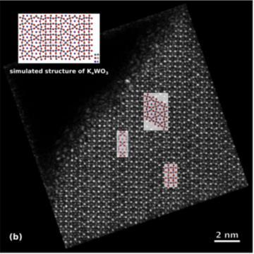
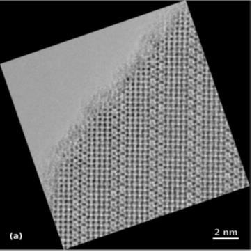
Fig. a) Conventional HRTEM image and b) recovered phase image for KxWO3 specimen
Fig. shows the comparison between original HRTEM image (acquired with JEOL JEM 3000F) and recovered phase image (obtained by K. Morawiec with his EWR software) of KxWO3 specimen. The latter shows much higher contrast and resolution than conventional HRTEM image. One can clearly distinguish potassium and tungsten sites, and in some areas even oxygen atoms are visible. Simulated structure of tungsten bronze was imposed on the phase image to validate obtained results. Future goal is to enhance resolution of reconstucted images so that oxygen atoms are clearly resolved.
Last but not least, during his visit K. Morawiec was acquainted with a group of PhD students involved in many aspects of the electron microscopy field (e.g. sample preparation, electron diffraction simulations, writing scripts for remote control of the microscope). He had an opportunity to observe their work and exchange experience gained in microscopy group at the Institute of Physics PAS.
- • Dr. hab. Eng. Anna Wolska, Dr. Marcin T. Klepka – Task 2.2 – Visit to European Synchrotron Radiation Facility
In the framework of task 2.2 of the work package "Enhancing of human potential through exchange of know-how and twinning activities with partnering organization" Dr. Anna Wolska and Dr. Marcin T. Klepka visited the European Synchrotron Radiation Facility, Grenoble, France in the period of June 10th - 17th, 2015.
The main goal of the visit was to perform X-ray absorption measurements of the thin Pt/Co/Pt trilayers within the accepted project: Local structure and residual strains induced distortion in Pt/Co/Pt trilayers after ultrafast electromagnetic irradiation. In this experiment the local structure around the cobalt atoms in thin magnetic layers was investigated by means of extended X-ray absorption fine structure (EXAFS) and X-ray absorption near edge fine structure (XANES) techniques.
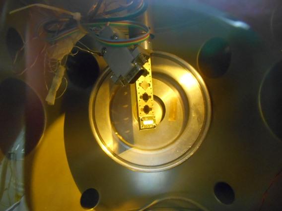
The XAFS signal was gathered in fluorescence mode in two configurations - perpendicular and normal to the beam by using the 12-element Ge detector. The samples were mounted in the cryostat which enabled measurements at low temperature (80K). The experiment was performed under supervision of Dr. Angela Trapananti.
- • Prof. Dr. hab. Tomasz Dietl, Prof. Dr hab. Roman Puźniak, Prof. Dr hab. Andrzej Wiśniewski – Task 2.7 - Visit to NCSR Demokritos, Institute of Nanoscience and Nanotechnology, Greece
In the framework of task 2.7 of work package "Enhancing of human potential through exchange of know-how and twinning activities with partnering organization" Prof. Dr. hab. Tomasz Dietl, Prof. Dr. hab. Roman Puźniak, Prof. Dr. hab. Andrzej Wiśniewski visited NCSR Demokritos, Institute of Nanoscience and Nanotechnology, Greece in the period of June 1st – 6th, 2015.
The goal of the visit was to discuss the scientific results, establishing of the scope of cooperation in studies of magnetic properties of core-shell (Ge,Fe)N antiferromagnetic-ferromagnetic nanostructures and manganites and cobaltites nanoparticles, participation in the meeting devoted to the achievements of COMANA project coordinated by NCRS Demokritos.
The Groups in the Institute of Physics headed by Prof. Dietl and Prof. Puźniak since few years study magnetic properties of (Cd,Mn)Te and (Ga,Mn)N epilayers (concluded by five joint publications) and of core-shell GeFeN antiferromagnetic-ferromagnetic nanocrystals and nanoparticles of manganites and cobaltites. On the other hand, the group of Prof. Trohidou from NCSR Demokritos has broad experience in the first-principle calculation of magnetic properties of core/shell nanostructures. During the visit new (unpublished) results were presented and possible scope of further cooperation was discussed. Cooperation between IF PAN and NCSR Demokritos on experimental and theoretical studies of magnetic nanostructures and nanoparticels was established. Profs. Dietl, Puźniak and Wiśniewski have also attended the workshop. The workshop has disseminated the scientific results obtained in the last 32 months by the COMANA project in the framework of the action “ARISTEIA” on the development of novel Complex Magnetic Nanostructures. Its aim was to bring together scientists and students from different research environments, actively involved in research on systems of complex nanostructures. The Workshop created great opportunities to discuss developments and establish contacts for initiating networks for future project submissions. During the workshop Prof. Dietl has delivered a talk: ”Spin dynamics in magnetic nanostructures: quantum vs. semiclassical approach”, Prof. Puźniak: “Particle Size Effect on Charge Ordering and Exchange Bias in (Sm,Ca,Sr)MnO3 Manganites”, Prof. Wiśniewski: “Pressure effect on ferromagnetism and exchange bias in Ru-doped manganites and La0.9 Ba0.1CoO3”. These invited talks presented recent results obtained at the Institute of Physics.
- • Prof. Dr. hab. Wojciech Paszkowicz and Dr. J. Domagała – Task 2.2 - Visit to Synchrotron Radiation Facility, Grenoble, France
In the framework of task 2.2 of work package "Enhancing of human potential through exchange of know-how and twinning activities with partnering organization" Prof. W. Paszkowicz and Dr. J. Domagała visited the Synchrotron Radiation Facility, Grenoble, France (ESRF) in the period of May 28th – June 23rd/27th, 2015.
 The delegates have visited the laboratories of ESRF, a 6-GeV synchrotron with multiple beamlines available for experimental studies. The visit included meetings with the staff and users of a number of beamlines and taking part in a seminar on X-ray imaging (2nd June 2015, by Dr. P. Cloetens) and measurements of crystallographic defects of the selected samples by topographical methods at BM05 beamline. Most attention was paid to the work of beamlines serving for diffraction measurements of various kinds. During the visit at the Microdiffraction Imaging Beamline (ID01, specialized in nanodiffraction, coherent diffraction, anomalous SAXS),recently upgraded, the delegates were particularly interested in the opportunities for measurement of semiconductor nanowires. Discussion with the staff of Surface and Interface X-ray Diffraction beamline (ID03) enabled understanding of multiple experimental opportunities offered there for experimental studies of the structure and morphology of surfaces and interfaces.
During the visit at the ID06 beamline, devoted to high-pressure diffraction studies of relatively large samples and to X-ray microscopy with spatial resolution of 100 nm, the visitors studied the experimental opportunities achievable at this beamline. The delegates have also learned the options available at the White Beam Beamline, High Pressure Station (ID09A) serving for studies of crystal structure at Extreme Conditions. Here the diffraction studies are possible in diamond anvil cells at pressures achieving several tens of GPa.
Prof. W. Paszkowicz (left), Dr. J. Härtwig (right), in the hutch of BM05 (X-ray Imaging and Optics Beamline.
 The High Resolution/High Throughput powder diffraction station (ID22) is equipped with a diffractometer devoted to powder diffraction studies at ambient and non-ambient temperatures ranging from 4 K to 1200/1500 °C. In the high-resolution option, ten counters with analyzers are used, resulting in an extremely high resolution of the collected data. The X-ray Imaging and Optics Beamline (BM05), The BM05 beamline has two experimental stations which can be used alternatively. One of the main purposes is the characterization of X-ray optics elements serving at other beamlines. It can also be used for studies of quality of single crystals. During the stay, experiments were performed on BM05 beamline in order to characterize selected nitride and oxide crystals, which are an object of studies in the Institute of Physics PAS, using X-ray topography methods.
During the stay, the delegates got acquainted with technical details of ESRF laboratories. This leads to an increase of qualification level of the delegates in the field of application of advanced synchrotron experimental techniques in crystallography and related fields. In particular, the visit helped in both, planning of future experimental studies with participation of IFPAN groups, and design of the future diffraction beamlines to be constructed at the Polish radiation source SOLARIS.
A view on the new large volume press at the ID06 Beamline.
- • Dr. Marcin T. Klepka, Dr. hab. Eng. Anna Wolska – Task 2.1 – Visit to Elettra, Sincrotrone Trieste
In the framework of task 2.1 of the work package "Enhancing of human potential through exchange of know-how and twinning activities with partnering organization" Dr. Marcin T. Klepka and Dr. Anna Wolska visited the Elettra synchrotron, located close to Trieste, Italy in the period of May 25th - 30th, 2015.
The goal of the visit was to continue learning about experimental set-up and capabilities of X-Ray Fluorescence experimental station by performing Grazing Incidence X-Ray Fluorescence (GI-XRF) and grazing incidence X-Ray Reflectometry (XRR) experiment with Dr. Diane Eichert - a research scientist at XRF beamline at Elettra. So far, the first test measurements performed in December 2014 revealed that Pt/Co/Pt thin layers fabricated at the IP PAS are the perfect materials to investigate by using these techniques. These preliminary results allowed to prepare a proposal for a beamtime which was accepted for the second part of 2015. (The XRF beamline opens for regular users in July 2015.)
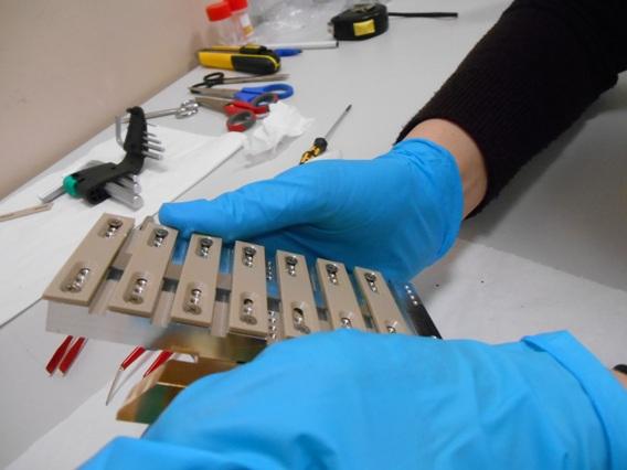
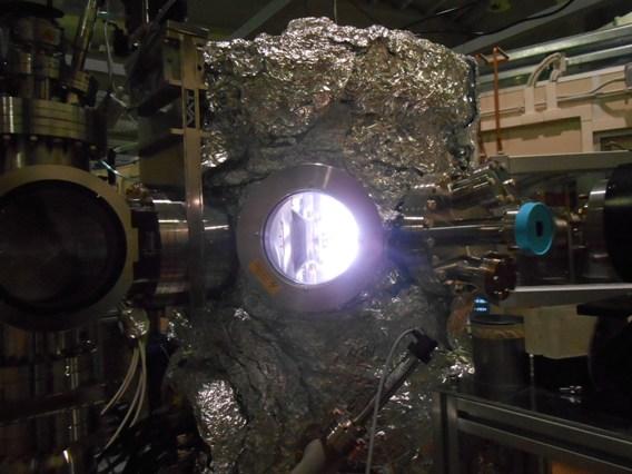
Since some doubts about the best method of the sample preparations appeared, few days of beamtime in May, for more test measurements during the commissioning time, were offered by Dr. Eichert. Additional measurements helped to clarify the concerns. Samples grown with different parameters were measured and the results were analyzed and compared. Furthermore, during our visit we have got more familiar with the beamline software and proper alignment of the samples. The analysis and understanding of the data were also discussed as well as particular details concerning further collaboration in the topic of structural investigations of thin layered systems.
- • Prof. Dr. hab. Wojciech Szuszkiewicz – Task 2.10 – Visit to CEA – Saclay, Gif-sur-Yvette, France
In the framework of task 2.10 of the work package "Enhancing of human potential through exchange of know-how and twinning activities with partnering organization" Prof. Dr. hab. Wojciech Szuszkiewicz visited CEA – Saclay, Gif-sur-Yvette, France in the period of May 17th - June 2nd, 2015.
During my stay at CEA Saclay I had an opportunity to visit a few neutron beamlines and to get acquainted with selected experimental details related to investigations of structure and magnetic properties of magnetic thin layers and multilayers with the use of polarized neutron reflectivity (PNR). I have learned about individual polarized neutron instrument progress and planned project’s upgrade. Moreover, I had an opportunity to visit the neutron scattering beamline dedicated to neutron imaging, being currently under construction. Dr. Frederic Ott - and an expert in polarized neutron reflectivity - has shown me and explained in details experimental possibilities offered by the PRISM spectrometer. This spectrometer is installed on a cold neutron beam. During the experiment one can apply magnetic fields up to 2 T and perform the reflectivity measurements below the room temperature as a function of temperature starting from about 10 K. Dr. Ott has shown me also the results of his last investigations, dedicated to neutron scattering studies of multilayers, applied as ‘supermirrors’ in several neutron scattering centers. The newest experimental results from PNR research got accepted for presentations during the International Conference on Magnetism ICM2015 in Barcelona (Spain). My attention was focused mainly at solid state physics, in particular in recent achievements in the area of semiconductor and metal physics.
My stay at LLB was also an excellent opportunity to perform the PNR test measurements. I took advantage of metallic magnetic multilayers containing Co, grown at IFPAN. Such multilayers are of important interest due to their possible applications in the area of information storage. The PNR measurements could complete presently available results of other studies like, e.g., XRD, EXAFS and MOKE, which were performed in the last year by the research team from IFPAN and from University of Białystok.
- • Dr. Iraida Demchenko, Dr. Yevgen Melikhov, Dr. Gennadiy Derkachov, MSc. Pavlo Konstantynov – Task 2.4 - Visit to ALBA - synchrotron light facility - Cerdanyola del Valles, Spain
In the framework of task 2.4 of work package "Enhancing of human potential through exchange of know-how and twinning activities with partnering organization" Dr. Iraida Demchenko, Dr. Yevgen Melikhov, Dr. Gennadiy Derkachov, MSc. Pavlo Konstantynov visited ALBA synchrotron light facility on March 17th - 24th, 2015.
The scientific goal of the research visit to the ALBA synchrotron light facility, more specifically CLAESS beamline, was to increase academic qualifications in the field of X-ray absorption spectroscopy in the framework of the finalization of the research project entitled "XAFS Investigations of local structural changes in (Ga,Mn)As thin layers at low temperature postgrowth annealing". In addition, discussions related to preparation of a joint FET Open grant application (H2020-FETOPEN-2014/2015: Novel ideas for radically new technologies) were planned to be conducted with top managerial staff of ALBA.
A series of meetings with the leaders of CLAESS beamline at ALBA synchrotron light facility were carried out in order to discuss particular details of continued from 2014 scientific project mentioned above. Our especial gratitude is for Dr. L. Simonelli (Beamline Responsible Officer), dr. C. Marini (Beamline Scientist), and Dr. W. Olszewski (PostDoctoral Research Associate). In order to finalize the research project, the new way of sample’s preparation was mastered which involved chemical separation of the investigated layer from the substrate. The preliminary analysis of the results of the measurements allowed us to propose the following working hypothesis: the process of annealing causes a bigger fraction of Mn to leave their original positions and to form more/bigger Mn-containing phases/clusters, showing that the material undergoes a local structural transformation around the Mn atoms. The detailed analysis of the results is currently being performed.
In addition to the finalization of the research project, two meetings were conducted with Dr. E. Pellegrin (EAgLE coordinator at ALBA) concerning IF PAN-ALBA twinning plan for 2015. Also, a meeting to discuss a potential joint grant application to FET Open was conducted with Prof. M. Aranda (Scientific Director), Dr. L. Simonelli (Beamline CLAESS Responsible Officer), O. Matilla (Head of Electronics Section) and Dr. E. Pellegrin (EAgLE coordinator at ALBA). We were informed that the decision of ALBA’s participation in the grant application will be made after discussions with dr. C. Biscari (ALBA's Director). The coordinator at IF PAN Dr. I. Demchenko should be notified by April 7, 2015 of their final decision.
The results obtained during realization of this project contribute to a deeper understanding of the meaning of the EXAFS parameters, stimulate further efforts to increase the accuracy of EXAFS experiments and data analyses, especially in case of samples with high order of inhomogeneity. The obtained experimental results point to possibilities, which are still little explored, of extracting original information on local dynamical properties of solids. Preparation and possible realization of a joint FET Open project would add a significant value for potential increase of research at the IF PAN.
- • Dr. Vitalii Ivanov – Task 2.13 - Visit to DUT, Dortmund, Germany
In the framework of task 2.13 of work package "Enhancing of human potential through exchange of know-how and twinning activities with partnering organization" Dr. Vitalii Ivanov visited DUT, Dortmund, Germany on March 5th - April 12th, 2015.
The current visit activity was a continuation of the program of trainings started during the previous visits to Dortmund TU
in December 2014. It included:
−training in the application of polarization resolved magneto-spectroscopy and nonlinear optical techniques to investigate
nanostructures of dilute magnetic semiconductors - quantum dots (QD) and quantum wells (QD);
−training in application of time-resolved Faraday rotation (TRFR) and time-resolved Kerr rotation (TRKR) spectroscopy
to investigation of semiconductors nanostructures (QD and QW).
Mainly, the efforts were focused on the measurements and determination of parameters of spin kinetic processes: spin relaxation and spin decoherency times in II-VI compounds based QD and QW. Using technique of TRKR and resonant spin amplification (RSA) CdMnTe/CdMgTe QW has been studied: dependence of spin decoherence time T2* on the Mn2+ ions content and photo-induced free carriers concentration were investigated. Also, using techniques of resonant second harmonic generation spin structure of excitons in ZnO monocrystals was studied.
Results of the experiments have been discussed with prof. M. Bayer, prof. D. Yakovlev and prof. E. Zhukov from DTU. Draft of the article “Mechanisms of spin-dependent energy transfer in (Zn,Mn)Se/(Be,Zn)Se and (Zn,Mn)Te/(Zn,Mg)Te DMS quantum wells” got advanced.
- • Dr. hab. inż. Anna Wolska, Dr. Marcin T. Klepka, and Dr. Paweł Rejmak – Task 2.1 - Visit to Elettra, Sincrotrone Trieste
In the framework of task 2.1 of work package "Enhancing of human potential through exchange of know-how and twinning activities with partnering organization" Dr. hab. inż. Anna Wolska, Dr. Marcin T. Klepka, and Dr. Paweł Rejmak visited the Elettra synchrotron, located close to Trieste, Italy in the period ofJanuary 29th - February 2nd 2015.
The goal of the visit was to get acquainted with the experimental conditions for the measurements of the liquid samples and to start collaboration with Dr. Giuliana Aquilanti - beamline scientist at XAFS station.
The test measurements were performed, at XAFS beamline at Elettra, on the Cu complexes of the coumarin derivatives. Complexes were prepared at the IP PAS in the form of microcrystalline powder. The solubility in DMSO and DMF was checked before experiment. The goal of the experiment was to test possibility of measurements in solutions using liquid cell. Our plan was to use transmission detection mode to get XAFS data for liquid samples. Unfortunately, it occurred impossible and changing detection mode to fluorescence was essential. Such mode required long acquisition time. Initial results indicated that number of near neighbour atoms is modified in comparison to microcrystalline powder. This can be linked with observed for that complexes antitumor and antibacterial activity. However, differences between used solvents were observed which will be the subject of further studies.

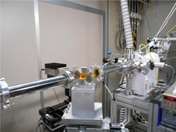
- • Prof. Dr. hab. Krystyna Jabłońska – Task 2.1 - Meeting with the director and scientists from FEL FERMI at Elettra
In the framework of task 2.1 of work package "Enhancing of human potential through exchange of know-how and twinning activities with partnering organization" prof. Krystyna Jablonska on 9th - 13th December 2014 was visiting the EAgLE scientific partner, Elettra synchrotron and free electron laser FERMI, located close to Trieste, Italy (fig.1).
The aim of the visit was discussing with Dr Maya Kiskinova, Dr Jacek Gajewski (NCBJ) and Dr Michele Svandrik director of FEL FERMI (fig.2), the procedure and details of the preparation of the common project for call TWINNING in program Horizon 2020 and participation in the workshop organizing by the Elettra “International Workshop on Advances in X-ray imaging” (fig.3). During the visit the fruitful discussion about the preparation of common project for TWINNING call with Dr Michele Svandrik, director of FERMI and Prof. Alfonso Francioso, Chief Executive Board of Elettra took place. The decision was taken about the involvement of free electron laser (FEL) FERMI in the project and range of FERMI participation was specified. On Friday 12th, during the visit at FERMI the detailed discussion with scientists from three working beamlines at this facility allowed to specify the fields of trainings to be offered by FERMI. The details of experiments and offered techniques were also explained. On 11 and 12 of December I took part in the “International Workshop on Advances in X-ray imaging” (Wsimaging). The detailed program and list of speakers of the workshop together with abstracts of presented lectures can be found at the webpage: http://www.elettra.eu/Conferences/2014/wsimaging/. The main topics of workshop were focussing on phase-sensitive X-ray imaging, synchrotron X-ray tomography, coherent X-ray imaging methods (with X-ray optics and/or lensless) and ultrafast time resolved imaging using FELs. Special attention was paid on progress in image analysis (reconstruction of 3D images and phase-retrieval algorithms) with reference to applications in different research fields, from medicine and biology to material science. Moreover, the visit provided also opportunity to discuss with Prof. Alfonso Francioso Poland participation in the CERIC-ERIC, the first material science ERIC consortium coordinated by Elettra.
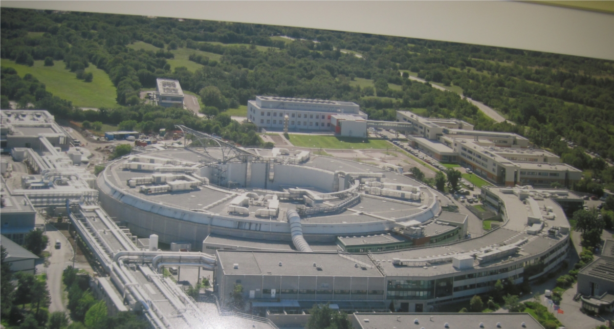
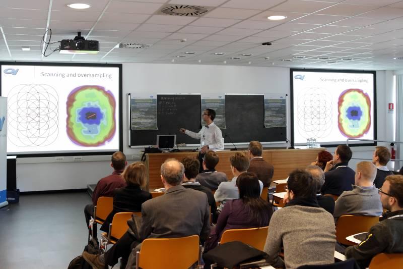
- • Prof. Dr. hab. Maciej Sawicki – Task 2.11 visit to University of Nottingham, UK
In the framework of task 2.11 of work package "Enhancing of human potential through exchange of know-how and twinning activities with partnering organization" Prof. Dr. hab. Maciej Sawicki visited University of Nottingham, UK in the period of December 14th - 17th, 2014.
During the visit, which was a direct continuation of the September 2014 visit of Nottingham’s Group of Spintronics and Ferromagnetic Semiconductors to IFPAN, a few meetings were held with members of the Group, the currently world leading inter-laboratory team investigating antiferromagnetic spintronics in I-II-V semiconductors such as LiMnAs and NaMnAs. Since the Nottingham group has recently commenced the growth of a new member of the AF semiconductor family which crystalizes in tetragonal symmetry: CuMnN, the talks were concentrated on the growth issues of this nitride compound as well as on challenges lying ahead of the proper assessment of its electrical and magnetic properties. It was agreed with prof. Bryan Gallagher that one member of IFPAN’s Group of magnetism of spintronic materials would join the Nottingham’s group for a long secondment (in the frame of the EAgLE’s twinning activity) to get fully acquainted with all the relevant and specific to this class of material techniques of material/structure processing, characterization and measurement. The provisional agreement says that the secondment should commence in early Spring 2015 and last about 12 months in total. The electrical measurements in Nottingham would be led and supervised by dr. P. Wadley whereas a possible synchrotron studies will be done with Dr. K. Edmonds.
As the result of the visit the latest information concerning the prospects of growth and join investigation of antiferromagnetic (Cu,Mn)N was gained and provisional agreement has been reached about a long lasting twinning based secondment of IFPAN stuff to Nottingham’s Group of Spintronics and Ferromagnetic Semiconductors.
- • Dr. Vitalii Ivanov – Task 2.13 - Visit to DUT, Dortmund, Germany
In the framework of task 2.13 of work package "Enhancing of human potential through exchange of know-how and twinning activities with partnering organization" Dr. Vitalii Ivanov visited DUT, Dortmund, Germany in December 7th - 23th, 2014.
During the stay in Dortmund Technical University (DTU) in the group of prof. Manfred Bayer following tasks were realized:
− training in the application of time resolved nonlinear-optical magneto-spectroscopy techniques to investigation on semiconductors
quantum dots (QD) and quantum wells (QD);
− training in application of time resolved Kerr rotation spectroscopy to study semiconductors nanostructures (QD and QW);
− characterization of novel semiconductors nanostructures (CdSe/ZnSe QD and ZnMnTe/ZnMgTe QW) which have been
manufactured recentlyin IFPAN (in the group of Prof. Jacek Kossut) using time resolved nonlinear-optics magneto spectroscopy.
Results obtained during the training and following experiments were discussed with Prof. M. Bayer, Prof. D. Yakovlev, and Prof. E. Zhukov from DTU. Draft of the article “Non-linear spectroscopy of Fano resonances in QD structures CdSe/ZnSe” has been prepared.
- • Dr. hab. inż. Anna Wolska, Dr. Marcin T. Klepka, Dr. Ryszard Sobierajski – Task 2.1 visit to Elettra synchrotron
In the framework of task 2.1 of work package "Enhancing of human potential through exchange of know-how and twinning activities with partnering organization" Dr. hab. inż. Anna Wolska, Dr. Marcin T. Klepka, Dr. inż. Ryszard Sobierajski visited the Elettra synchrotron, located close to Trieste, Italy in the period of November 30th - December 10th, 2014.
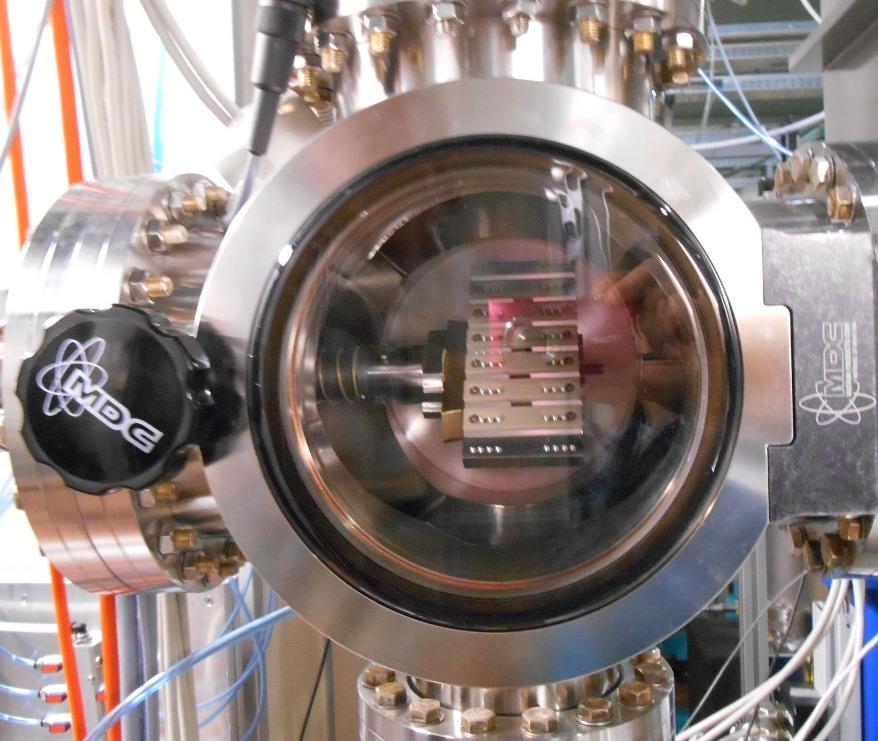
The goal of the visit was to get acquainted with the measurements technique of Grazing Incidence X-Ray Fluorescence (GI-XRF) and grazing incidence X-Ray Reflectometry (XRR) through the experiment with Dr. Diane Eichert - a research scientist at XRF beamline at Elettra. The test measurements were performed on Pt/Co/Pt thin layers fabricated at the IP PAS. Two types of samples were investigated: as-grown (with an in-plane magnetisation) and irradiated by intense extreme UV nanosecond pulses (with out-of-plane magnetisation). The purpose of the study was to correlate the observed magnetic changes with structural ones. The data for the as-grown samples showed very high quality layers with sharp interfaces, while in the irradiated ones high level of atomic intermixing was noticed. The detailed analysis and understanding of the data is one of the topics of further collaboration.
 During our visit we have got acquainted with the XRF beamline instrumentation, samples selection’s rules, applied measurement’s and basis of data analysis techniques. We have also learned about possible applications of the GI-XRF technique to study the structure of the thin layers.
Furthermore, we have got familiarized with the scientific research performed by the XRF group at Elettra and planned with Dr. Diane Eichert particular details concerning further collaboration in the topic of structural investigations of thin layered systems.
- • Prof. Dr. hab. Maciej Sawicki – Task 2.16 – Visit to HZDR Helmholtz Centrum Dresden, Rossendorf Institute of Ion Beam Physics and Materials Research
In the framework of task 2.16 of the work package "Enhancing of human potential through exchange of know-how and twinning activities with partnering organization" Prof. Maciej Sawicki visited HZDR Helmholtz Centrum Dresden Rossendorf, Institute of Ion Beam Physics and Materials Research between November 17th – 23rd, 2014.
The aim of the visit was to acquire knowledge on GaAs-like samples containing Mn preparation for electrical and magnetic measurements.
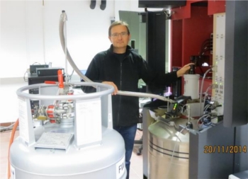 During the visit at the HZDR Helmholtz Centrum Prof. Sawicki discussed with the head of the Institute Prof. Manfred Helm and Dr. Shengqiang Zhou the recent experimental findings in magnetotransport and direct magnetization measurements in various derivatives of GaAs host semiconductor (that is InGaAs, GaAsP, InAs, and GaP) with Mn, putting the main emphasis on experimentally correct assessment of the magnetic properties of the studied compounds. There has been an increasing concern about the true nature of the hole states which mediate the Mn-Mn ferromagnetic coupling in (Ga,Mn)As and a dedicated studies of relative to GaAs compounds may, or even should, shed light on this issue. In particular, a lot of attention was put on the sample preparation procedure in which ion implantation and ultra-fast laser pulses are in use for sample recrystallization. It has been agreed that samples prepared by this way will be shipped to IFPAN for magnetization studies. Also, already existing GaN layers with Mn will be treated in a similar way in HZDR in order to promote the carrier mediated ferromagnetic Mn-Mn coupling in (Ga,Mn)N.
Prof. Sawicki also delivered a talk in a series of Institute Colloquiums entitled: „The origin of ferromagnetism and critical behavior in insulating (Ga,Mn)N” during which an introduction to the objectives of the EAgLE project reinforced collaboration was given.
- • Dr. Iraida Demchenko, Dr. Yevgen Melikhov – Visit to ELETTRA synchrotron radiation facility in Trieste (Italy)
In the framework of Task 2.1 of work package "Enhancing of human potential through exchange of know-how and twinning activities with partnering organization" Dr. I. Demchenko and Dr. Y. Melikhov visited ELETTRA synchrotron radiation facility in Trieste (Italy) in the period of November 10th - 17th, 2014.
The scientific goal of the research visit to the ELETTRA synchrotron, X-Ray Fluorescence beamline (10.1L), was to increase academic qualifications in the field of X-ray Spectrometry Techniques such as Grazing Incidence X-Ray Fluorescence (GI-XRF), Total Reflection XRF (TXRF), and X-Ray Reflectometry (XRR) through the realization of research project entitled "GI-XRF and XRR investigations of local structural changes in (Ga,Mn)As thin layers at low temperature postgrowth annealing".
The continuous downscaling of the process size for semiconductor devices pushes the junction depths and consequentially the impurity depths in the host matrix, which in its turn motivates the need for sensitive methods capable of analyzing dopant distribution and possible impurities. In this context a series of meetings with the leader and scientists of 10.1L beamline at ELETTRA synchrotron were carried out in order to discuss particular details of mentioned above research project. After initial discussions dealing with the priority of following GI-XRF and XRR measurements, the applicability of both techniques was demonstrated for (Ga,Mn)As thin layers devoting particular attention on the tricks to perform successful and reliable measurements with attention to future interpretation of obtained data. Thus, XRR is an established technique for the characterization of single- and multi-layered thin film structures with layer thicknesses in the nanometer range. XRR spectra are acquired by varying the incident angle in the grazing incidence regime while measuring the specular reflected X-ray beam. The shape of the resulting angle-dependent curve is correlated to changes of the electron density in the sample, but does not provide direct information on the presence or distribution of chemical elements in the sample.
GI-XRF measures the XRF induced by an X-ray beam incident under grazing angles. The resulting angle dependent intensity curves are correlated to the depth distribution and mass density of the elements in the sample. GI-XRF provides information on contaminations, elements content and to some extent on the depth of the dopant distribution, but is ambiguous with regard to the exact distribution function.
Both techniques use similar measurement procedures and data evaluation strategies, i.e. optimization of a sample model by fitting measured and calculated angle curves. Moreover, the applied sample models can be derived from the same physical properties, like atomic scattering/form factors and elemental concentrations; a simultaneous analysis is therefore a straightforward approach. This combined analysis in turn reduces the uncertainties of the individual techniques, allowing a determination of content and depth profile of the doped elements with drastically increased confidence level.
Our especial gratitude belongs to Diane EICHERT, Beamline Coordinator, Werner JARK, Beamline Scientist, and Fabio BRIGIDI, PostDoctoral Research Associate, who were able to pass their knowledge in an interesting, friendly and professional manner.
X-ray techniques utilizing the external reflection of X-rays are very surface sensitive, hence providing a non-destructive tool for process analysis and control of sample quality. The results obtained during realization of this project contributes to a deeper understanding of GI-XFR and XRR measurement techniques and their related parameters. This includes not only ability to follow the procedure and to perform experiments but also a focused data analysis. All of that adds significant value for potential increase of research at the IP PAS.
- • Prof. Dr. hab. Maciej Sawicki – Task 2.6 – Visit to University of Wuerzburg, Experimentelle Physik III, Wuerzburg, Germany
In the framework of task 2.6 of the work package "Enhancing of human potential through exchange of know-how and twinning activities with partnering organization" Prof. Maciej Sawicki visited University of Wuerzburg, Experimentelle Physik III, Wuerzburg, Germany between November 2nd – 5th, 2014.
The aim of the visit was to acquire the knowledge on lithographic structuring and electrical contacting of epitaxial layers of Bi2Se3 doped with Cr – a topological material of a great interest to the IFPAN community and MnSi – a new spintronic material.
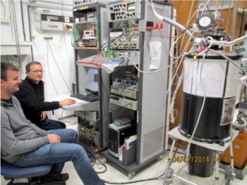 During the visit at the University of Wuerzburg Prof. Sawicki discussed with the head of the lab Prof. Laurence Mollenkamp and Dr. Charles Gould the recent experimental findings in magnetotransport measurements in Cr-doped of Bi2Se3 and magneric measurements of epitaxial layers of MnSi. He also took part in a nanospintronics group meeting where new results of unexpected millikelvin properties of some of the layers were presented. As little is understood at the very moment various issues related to sample preparation, their handling during the experiment and the data analysis were discussed and the plans were laid for further experimental effort to resolve this interesting issue. It has been agreed that some experiments will be performed by visitors from Wuerzburg at IFPAN at near future under the support of the EAgLE project.
As there remained a small possibility that this unexpected behaviour might have been due to a presence of some accidental ground loops or misconducting of the low temperature experiment a hands-on check-up of the experimental set up at Wuerzburg was conducted. As no obvious flaws were identified, the decision was made to carry on with further investigation of this effect.
- • Prof. Dr. hab. Maciej Sawicki – Task 2.5 – Visit to Institute of Solid State Physics, University of Bremen, Germany
In the framework of task 2.5 of the work package "Enhancing of human potential through exchange of know-how and twinning activities with partnering organization" Prof. Maciej Sawicki visited Institute of Solid State Physics, University of Bremen, Germany between October 20th – 26th, 2014.
The goal of the visit was to elaborate a suitable methods and routines of structural characterization and growth techniques of a new spintronics material: antiferromagnetic CuMnN.
 Recent studies have demonstrated the potential of antiferromagnets as the active component in spintronic devices. This is in contrast to their current passive role as pinning layers in hard disk read heads and magnetic memories. The choice of ternary system CuMnN stems mainly from the fact that its tetragonal symmetry should enhance the magnetocrystalline anisotropy phenomena and so makes it favorable for the concept of spintronics.
The visit was hosted by Dr. Gerd Kunert with who most of the discussions and scientific interaction took place. However, during the visit numerous discussions took place with other members of the Semiconductor Epitaxy Group, including its head, Prof. D. Hommel. One of the main topics of the discussions were means of determination of the spin arrangement in this material. It was agreed that for the time being the main emphasis will be put on the conventional x-ray diffraction performed in Bremen, Rutherford backscattering spectrometry to be performed in HZDR Rozendorf-Dresden, and secondary ion mass spectrometry and SQUID magnetometry to be performed at IFPAN.
- • Dr. Katarzyna Gas – Task 2.5 – Visit to Institute of Solid State Physics, University of Bremen, Germany
In the framework of task 2.5 of the work package "Enhancing of human potential through exchange of know-how and twinning activities with partnering organization" Dr. Katarzyna Gas visited Institute of Solid State Physics, University of Bremen, Germany between October 14th – 26th, 2014.
The goal of the visit was to get further acquainted with advanced methods of MBE growth Mn-doped GaN epilayers for spintronics applications.
 This visit was the continuation of the previous one, held between 13th and 21st of September, 2014 and this time the main emphasis was shifted towards mastering the already acquainted skills concerning the methods of molecular beam epitaxy (MBE) growth of semiconductor structures consisting ultra-thin layers of manganese doped gallium nitride.
During the visit Dr. Gas participated in the MBE growth of different nanostructures containing of GaN:Mn epilayers. The samples were grown in EPI930 MBE chamber equipped with a RF-plasma source on GaN templates prepared by metal-organic vapor-phase epitaxy on sapphire substrates. The first set of samples constituted heterostructures consisting of GaN:Mn thick buffer layer with low Mn concentration, GaN:Mg layer with various Mg concentration and finally thin GaN:Mn layer with substantial amount of Mn. The first, weakly Mn doped layer serves as the buffer for the further growth and the addition of Mn aims to make this buffer insulating. Such heterostructures are of the main interests for IFPAN scientists and will be further investigated by the group of profs. T. Dietl and M. Sawicki. The second type of samples were thin GaN layers co-doped with arsenic and manganese. Some attempts were made to optimize such a growth (substrate temperature, elementary fluxes). This was the first, necessary step for more substantial incorporation of both Mn and As to the GaN matrix which is expected to acquire p-type conductivity promoting the ferromagnetic coupling described by Zener model. After the growth the samples were investigated by high resolution X-ray diffraction. These measurements allowed to assess their crystal quality as well as to determine the Mn concentration. The samples’ thicknesses were determined by using scanning electron microscopy.
- • Dr. Jarosław Domagala and dr. Roman Minikayev – Task 2.4 – Visit to ALBA Sincrotrone, Cerdanyola del Vallès near Barcelona, Spain
In the framework of task 2.4 of the work package "Enhancing of human potential through exchange of know-how and twinning activities with partnering organization" Dr. J. Domagała and Dr. R. Minikayev visited the ALBA synchrotron, located close to Barselona, Spain in the period of October 13th - October 20th, 2014.
The scientific goal of the research visit to the ALBA synchrotron, high-resolution powder diffraction and high pressure powder diffraction beamline BL04 - MSPD, was to increase academic qualifications in the field of high pressure x-ray powder diffraction in the framework of the realization of research project entitled "Equation of state of whitlockite-related vanadates". During the visit a series of meetings with the leaders of MSPD beamline at ALBA synchrotron were carried out in order to discuss particular details of accepted for realization scientific project mentioned above. Dr Domagala and Dr Minikayev got acquainted with the details of the operation of the beamline and how to optimize the synchrotron beam (the photon energy, mono-chromatization, focusing optics). Special gratitude is for Francois Fauth Beamline Responsible Officer, Catalin Popescu Post-Doctoral Research Associate. The experiments were performed on the MSPD endstation at room temperature and high pressure (up to 20Gpa) conditions. The beamline staff demonstrated several new techniques of sample loading into modern diamond anvil cell camera which is a corner stone of successful high pressure experiment. The experimental setup calibration procedure and efficient arrangement of the pressure gauge made the insitu measurements precise and short time.
The obtained experimental results provided structural data of the whitlockite-type compounds in a set of high pressure ranges, still missing in the literature. The knowledge of elastic properties of these materials is of importance for the potential applications in optoelectronics.
- • Dr. Katarzyna Gas – Task 2.5 – Visit to Institute of Solid State Physics, University of Bremen, Germany
In the framework of task 2.5 of the work package "Enhancing of human potential through exchange of know-how and twinning activities with partnering organization" Dr. Katarzyna Gas visited Institute of Solid State Physics, University of Bremen, Germany between September 12th – 21st, 2014.
The goal of the visit was to get acquainted with methods of molecular beam epitaxy (MBE) growth of thin layers of manganese doped gallium nitride - diluted magnetic semiconductor with promising applications in the field of semiconductor spintronics.
 During the first day of the visit at Institute of Solid State Physics dr Gas became acquainted with the experimental equipment of the Semiconductor Epitaxy Group main laboratories such as high-resolution X-ray diffractometer (Philips X'Pert MRD), Hall effect measurement setup, micro-photoluminescence setup, focused ion beam and scanning electron microscope, and atomic force microscope.
The majority of the time the visitor spent in MBE growth laboratory where the detailed familiarization with the principles of operating of 3-chamber molecular epitaxy MBE "EPI 930" system took place. The system consists of one reactor for group-III-Nitrides and GaAs, one reactor for ZnSe and derivatives, and an XPS-analysis chamber. The reactors are equipped with rf-plasma cell, ellipsometry, high resolution RHEED camera and quadruple mass spectrometer. The sapphire substrate preparation techniques used to MBE – growth of GaN thin layers as well as the post processing of the samples have been learnt. Numerous discussions with Bremen team (most frequently with Dr. Gerd Kunert, the direct supervisior of Dr. Gas visit) helped to establish the necessary growth conditions for efficient incorporation of Mn dopant to the GaN matrix during the MBE growth, allowing for maximization of the Curie temperature in (Ga,Mn)N layers.
- • Dr. Iraida Demchenko, Dr. Yevgen Melikhov, Dr. Anastasiya Derkachova – Visit to ALBA- synchrotron light facility - Cerdanyola del Valles, Spain
The scientific goal of our research visit to the ALBA synchrotron, beamline CLAESS, on September 10th - 17th, 2014 was to strengthen our academic qualifications in the field of x-ray absorption spectroscopy in the framework of the realization of research project entitled "XAFS Investigations of local structural changes in (Ga, Mn) As thin layers at low temperature postgrowth annealing".
In the framework of work package 2 "Enhancing of human potential through exchange of know-how and twinning activities with partnering organization" of the EAgLE project, a series of meetings with the leaders of CLAESS beamline at ALBA synchrotron were carried out in order to discuss particular details of accepted for realization scientific project mentioned above. It is worth mentioning that everyone we worked with was an excellent specialist in his/her field and was able to pass knowledge in an interesting and friendly manner. Our especial gratitude is for Laura Simonelli, Beamline Responsible Officer, Carlo Marini, Beamline Scientist, and Wojciech Olszewski, PostDoctoral Research Associate. Overall, the time spent at the CLAESS beamline was enjoyable and fruitful, we have seen fascinating machines, learned an incredible amount of scientific details about how the mentioned beamline functionates and gained quite many new skills as well as developing those already possessed.
This collaboration significantly extends our knowledge about the design and construction of the 'X-ray spectroscopy' experimental station built in Krakow for Solaris synchrotron facility. Moreover, we expect that the results obtained during realization of our project should contribute to a deeper understanding of the EXAFS parameters meaning , and stimulate further efforts to increase the accuracy of EXAFS experiments and data analysis.
- • Dr. hab. inż. Anna Wolska, Dr. Marcin T. Klepka – Visit to European Synchrotron Radiation Facility
In the framework of task 2.2 of work package "Enhancing of human potential through exchange of know-how and twinning activities with partnering organization" Dr. Anna Wolska and Dr. Marcin T. Klepka visited the European Synchrotron Radiation Facility, Grenoble, France in the period of September 8th - 19th, 2014.
First part of the visit was devoted to learning about the experimental set-up and possibilities of the beamline BM08 under the supervision of Dr. Angela Trapananti. The BM08 beamline is a standard X-ray absorption beamline on a bending magnet source. The beamline operates within very long energy range (4.0 - 90.0 keV) and is equipped with the Ge detectors which allows to gather a good quality signal for diluted samples. At this beamline the X-ray absorption measurements within the accepted project: Polarized XAFS study on the ion irradiated Me1/Co/Me2 (where Me1,Me2=Au,Pt) structures exhibiting perpendicular magnetic anisotropy were performed. In this experiment the local structure around the cobalt atoms in thin magnetic layers was investigated by means of extended X-ray absorption fine structure (EXAFS) method in fluorescence mode.
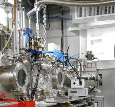
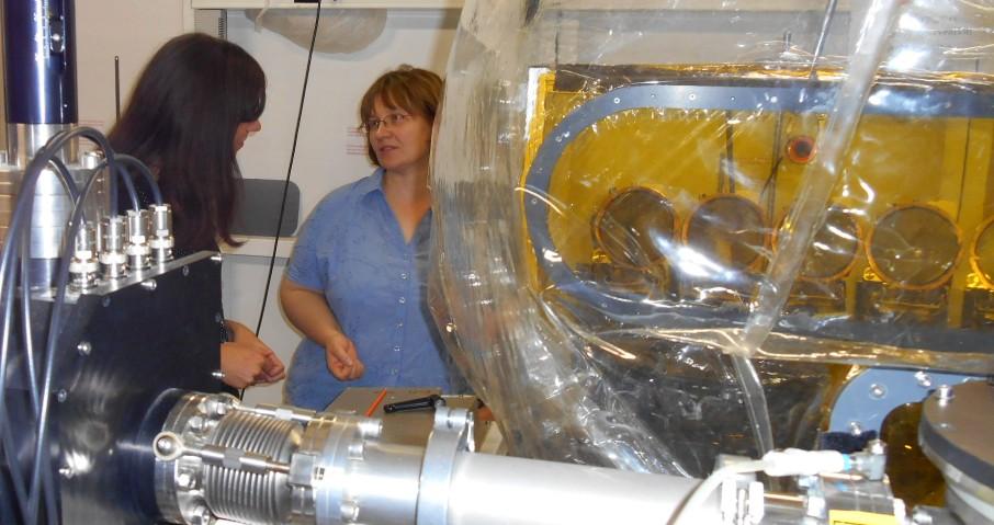
The visitors also met with Dr. Sara Lafuerza at beamline ID26. She showed and explained the experimental set-up of the beamline which is the high brilliance X-ray spectroscopy beamline equipped with an X-ray emission spectrometer. At this beamline X-ray absorption as well as X-ray emission spectroscopy experiments can be performed. Moreover, the high-brilliance X-ray beam allows for absorption studies on very diluted samples. The visitors also talked with Dr. Sakura Pascarelli - a scientist in charge of beamlines ID24 and BM23. She demonstrated and explained the experimental set-up for both of them. BM23 is a beamline for standard X-ray absorption measurements. On the other hand, beamline ID24 is a very modern experimental station where time-resolved and extreme conditions X-ray absorption spectroscopy experiments can be performed.
- • Prof. Dr. hab. Maciej Sawicki – Task 2.6 – Visit to University of Wuerzburg, Experimentelle Physik III, Wuerzburg, Germany
In the framework of task 2.6 of the work package "Enhancing of human potential through exchange of know-how and twinning activities with partnering organization" Prof. Maciej Sawicki visited University of Wuerzburg, Experimentelle Physik III, Wuerzburg, Germany between July 24th –August 1st, 2014.
The aim of the visit was to acquire the knowledge on lithographic structuring and electrical contacting of epitaxial layers of Bi2Se3 doped with Cr – a topological material of a great interest to the IFPAN community and MnSi – a new spintronic material.
During the visit at the University of Wuerzburg prof. Sawicki had a number of discussions with prof. L. Molenkamp, dr Ch. Gould and dr C. Brüne during which a number of issues related to sample preparation, their handling during the experiment and the data analysis were discussed.
Concerning the epitaxial layers of Bi2Se3 doped with Cr the main subject of the discussions was a poor relation between electrical and magnetic long time relaxation measurements in the ferromagnetic phase of 6 nm thin layer. Various models were considered and relevant ways of circumvent of the foreseen obstacles were proposed. As the results additional magnetic relaxation measurements were performed for the sample before and after chemical etching in HCl. Also, additional XRD measurements were scheduled. Finally, it was elaborated that an extreme care must be executed during electrical measurements which turned out to be prone to produce false results when electrical leak was present anywhere in the experimental setup.
The main discussions concerning the epitaxial layers of MnSi on Si(111) were related to the profound difficulties in obtaining error-free low temperature data for this system. Various attempt were made to solve the problem – mainly by changing the SQUID experimental routine and/or by changing the sample holder. The problem has been solved only for in-plane configuration for which a Si-based sample holder proved to be a sufficient solution. The other, perpendicular configuration, remained to be solved.
- • Dr. hab. Sławomir Kret – Task 2.3 – Visit to Department of Physics, University of Warwick, United Kingdom
In the framework of task 2.3 of the work package "Enhancing of human potential through exchange of know-how and twinning activities with partnering organization" Dr. hab. Sławomir Kret on 1 July to 15 July 2014 visited the EAgLE scientific partner Department of Physics, University of Warwick, United Kingdom.
During the visit the performance of a double aberration corrected transmission electron microscopy Jeol 200F was tested. This microscope is equipped with a dedicated probe corrector. Correction of aberration of the illuminating system gives opportunity of better focusing of the electron beam. For this reason achievement of 80 pm resolution is possible at 200 kV (for comparison whiteout this probe corrector Titan microscope installed in IFPAN can achieve only 136 pm resolution at 300 kV). With assistance of dr Ana Sanchez a series of test of HR-STEM and EDS performance was performed using corrected probe with high current density for PbTe/CdTe heterostructure and ZnTe/CdTe MBE grow nanowires. Also, different acquisition schemes were tested to improve signal to noise ratio. Finally, the influence of different source of the noise and interference during STEM acquisition was tested. For this purpose the Fourier analysis was performed. Initial analysis confirmed very high stage and environmental stability of JEO ARM installed in Warwick laboratory. Performed test and analysis will have an effect in optimization and task sharing of the common experiments performed in two labs on JEO ARM (Warwick) and FEI –Titan (IFPAN).
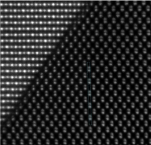
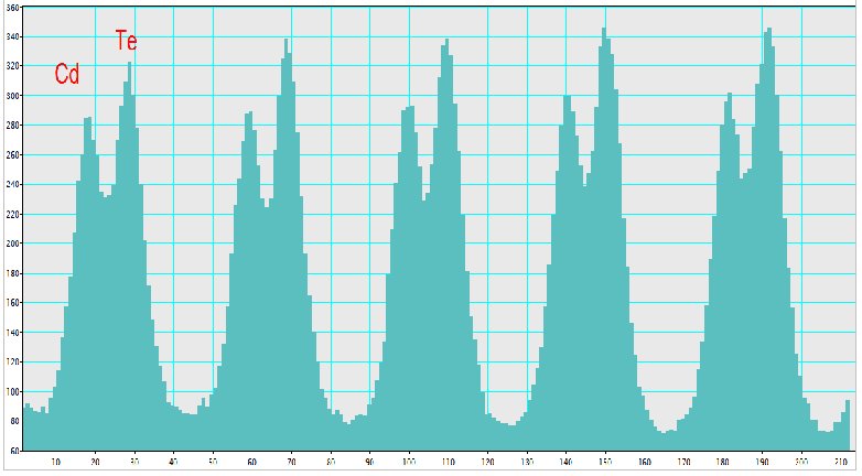
High contrast Cs-HRSTEM of CdTe/PbTe obtained on Jeol Arm 200F microscope as a sum of 20 individual images obtained with high speed scanning. Line profile reveals clearly difference of the contrast of Cd and Te atomic columns.
- • Dr. hab. Piotr Dłużewski – Task 2.3 – Visit to Department of Physics, University of Warwick, United Kingdom
In the framework of task 2.3 of the work package "Enhancing of human potential through exchange of know-how and twinning activities with partnering organization" Dr. hab. Piotr Dłużewski from 20 June to 3 July 2014 visited the EAgLE scientific partner Department of Physics, University of Warwick, United Kingdom.
I was hosted by Dr. Richard Beanland and Dr. Ana Sanchez. He showed me facility of transmission electron microscopy group and arranged meeting with PhD students, next he arranged discussions with dr Neil Wilson and dr Jeremy Slona. One of the most important aspect of the visit was discussion about problem of exit electron wave reconstruction (EWR) from series of defocused images. PhD student Adam Dyson developed unique software solving the reconstruction problem with a use of modern computation techniques, which dramatically speedup computing time need for the reconstruction. He presented the results in thesis “Advances in Computational Methods for Transmission Electron Microscopy Simulations and Image processing”. The usefulness of such a solution is extremely important for testing thin specimens by transmission electron microscopy. In this situation microscope images do not submit the actual structure of the object, but they are Fresnel diffraction Result. Useful information contained in the phase of the wave function of the electron beam, which penetrated preparation. Restoration phase is possible by using different algorithms, but so far these time-consuming calculations impossible to obtain reliable results in real time. The other discussion I did with Prof. Jeremy Slona who is the word leader in an investigation of structure of two-dimensional crystals embedded in single-wall carbon nanotubes (SWCNT). The discussions leaded us to the conclusion about reasonableness of making an observation of two-dimensional crystals embedded in SWCNTs with a use of 300 kV electron beam. The idea of that experiment coming from assumption that heavy atoms constituting the crystals will be better visible for higher energy electrons unlike in the case of the lower energy electrons applied for a visualization of the light carbon atoms constituting SWCNT. It was predicted that during prof. Slonas' visit in Warsaw such observations will be done with the use of Titan-Cubed 300 kV transmission electron microscope.
- • Prof. Dr. hab. Wojciech Paszkowicz – Visit to ALBA-CELLS Synchrotron
In the framework of task 2.4 of the work package "Enhancing of human potential through exchange of know-how and twinning activities with partnering organization" Prof. W. Paszkowicz visited the ALBA-CELLS Synchrotron, Cerdanyola des Valles / Barcelona, Spain. The visit took place in the period of 6th May – 2nd June, 2014.
The delegate has visited the laboratories of ALBA-CELLS. The visit included a meeting with the Director of ALBA, prof. M. Aranda, multiple visits and discussions with the staff of the MSPD, MISTRAL and XALOC beamlines as well as observation of sample preparation and run of measurements at these beamlines. ALBA-CELLS is a newly built 3-GeV synchrotron with seven beamlines constructed in the first phase, and with an opportunity to build a larger number of beamlines in the following phases. Most attention was paid to the work of the MSPD Materials Science and Powder Diffraction beamline. An inspection during a shutdown period enabled familiarizing with the beamline construction and optics. This beamline has two experimental stations which can be used alternatively: a High Pressure/Microdiffraction station and a High Resolution/High Throughput powder diffraction station. It is equipped with a three-circle diffractometer. In the high-resolution option, thirteen counters with analyzers are used. For the high-pressure and cultural-heritage related experimental studies, the X-ray optics is used ascertaining focus at the sample of the size of the order of 10x15 microns. In the high-pressure mode of operation, this optics enables diffraction studies in diamond anvil cells at pressures achieving several tens of GPa. The delegate has also visited a laboratory serving for preparation of samples for high-pressure experiments and observed the preparation of the high-pressure experiments.
 During the stay, the delegate has visited the MISTRAL beamline devoted to X-ray microscopy; this beamline served mostly for studies of biological samples. This beamline is devoted to cryotomography for biological applications. An important applicatio is visualisation of individual cells with a high resolution. The delegate has also visited the XALOC beamline devoted to macromolecular crystallography, At this beamline, most work is directed toward solving the protein structure. There is a high demand for studies at this beamline, connected with the importance of synchrotron radiation in biology, medicine and pharmaceutical industry. In summary, the delegate became acquainted with the construction and work of experimental diffraction beamline in the ALBA-CELLS synchrotron and of other selected beamlines running at this synchrotron. The visit will be useful, In particular, in the future work on design of a diffraction beamline at the Polish radiation source SOLARIS.
A view of the ALBA-CELLS building.
- • Prof. Zbigniew R. Żytkiewicz – Visited Institute of Solid State Physics - Semiconductor Epitaxy of University of Bremen
In the framework of task 2.5 of work package "Enhancing of human potential through exchange of know-how and twinning activities with partnering organization" Prof. Zbigniew R. Żytkiewicz and Ms. Marta Sobańska visited Institute of Solid State Physics - Semiconductor Epitaxy of University of Bremen, Bremen, Germany in the period of May 5th - 9th, 2014.
The goal of the visit was to get acquainted with methods of MOVPE growth of GaN nanowires on sapphire substrates and their further processing as well as with Mn doping during PAMBE growth of planar GaN epilayers. During the tour through the main laboratories of the Semiconductor Epitaxy group the visitors discussed with Prof. K. Sebald details of micro-photoluminescence studies of GaN nanowires and with Prof. J. Gutowski growth and application of ZnO nanowires. Majority of the time was spent in MBE and MOVPE growth laboratories and clean-rooms equipped with systems used for processing of semiconductor structures. The visitors got familiarized with the recipe used to cover nanowires with an optically transparent plastics prior to deposition of upper metallic contact. Chemistry and technological steps involved are very simple, thus the transfer of this technique to IF PAN laboratory is planned. The visitors also participated in MBE growth of Mn-doped GaN epilayers to learn what were the growth conditions necessary for efficient incorporation of Mn dopant to the GaN matrix during PAMBE epitaxy. Finally, Prof. Zytkiewicz gave the seminar talk entitled “Plasma-assisted MBE growth of GaN nanowires” presenting results of the IF PAN group on the PAMBE growth and studies of self-induced GaN nanowires.
- • Dr. Katarzyna Gas – Visit to French Atomic Energy Commission (CEA) – Saclay, France
In the framework of task 2.10 of work package "Enhancing of human potential through exchange of know-how and twinning activities with partnering organization"Dr. Katarzyna Gas visited CEA Saclay, France between March 30th and April 13th, 2014.
The aim of the visit was to get acquainted with advanced neutron spectroscopy techniques and their application to newly developed at IF PAN functional (thermoelectric and spintronics) materials.
During the first few days of the visit at Saclay Institute of Matter and Radiation (IRAMIS), dr. Gas got introduced to details of both the elastic and inelastic neutron scattering techniques and became acquainted with experimental facilities connected to the Orphée reactor. The former experimental technique allows to determine the atomic and/or magnetic structure of a material. The latter method is particularly effective in studies of collective excitations in condensed matter.
As a part of the training scheme she was involved in measurements of neutron diffraction on bulk crystals conducted by the experienced scientists of the host laboratory: dr Sylvian Petitt and Patrick Barroni. This also involved the whole course of sample mounting and alignment methods and data acquisition. The elastic scattering experiments were performed using a pioneering two-dimensional neutron detector Barotron, which was devised and constructed in the visited laboratory. The second type of measurement were devoted to the material brought from IF PAN, which was subjected to inelastic neutron scattering studies. This set-up, a triple axis spectrometer G 4-3 installed on the thermal neutron beamline of Orphée reactor, allows to obtain high resolution results despite the low energy of the neutrons and is particularly useful for measurements of dispersion curves of phonons and magnons, phonon softening, etc... On the other hand it serves well for elastic studies on problems where good peak/background ratio, suppression of inelastic scattering, high resolution of momentum and/or energy transfer are essential. ZnO, PbTe, and PbCdTe of various Cd composition were investigated. In particular, for ZnO bulk crystals temperature dependent studies were performed allowing for the first time accurate determination of the temperature dependence of phonon dispersion of this material.
|
| 
|
- • Prof. Ewa Jędryka, and Prof. Marek Wójcik – Visit to the Institut de Ciència de Materials de Barcelona (ICMAB-CSIC) , Bellaterra, Spain.
In the framework of task 2.12 of work package "Enhancing of human potential through exchange of know-how and twinning activities with partnering organization" Prof. Ewa Jędryka and Prof. Marek Wójcik visited the EAgLE scientific partner, prof. J. Fontcuberta a head of the research group “Multifunctional Oxides and Complex Structures” in the Institut de Ciència de Materials de Barcelona (ICMAB-CSIC), Bellaterra, Spain, in the period: February 24th – March 9th, 2014.
The purpose of this visit was to discuss the experimental results recently obtained in IF PAN on thin films of half doped La0.5A0.5MnO3 (A=Sr, Ca) manganites grown in ICMAB.
Half doped manganites have recently attracted renewed attention because their ground state can be modified by engineering the bandwidth or modifying their carrier density. This property makes them ideal materials for integration in reconfigurable ferroelectric tunnel junction with potentially large tunnel electro-resistance effect. The 55Mn NMR results obtained in IFPAN on La0.5Sr0.5MnO3 thin film series, 20 nm thick, including the samples on LSAT, STO and YAO substrates, which represent various degree of lattice mismatch were discussed along the results of XRD, magnetization and resistivity measurements obtained by the ICMAB group. The experimental data of the two groups were discussed in the context of the theoretical phase diagram of the ground state of manganites as a function of tetragonal distortion of their perovskite structure. 55Mn NMR data have revealed that the experimental ground state of the strained manganite films is not homogenous but it is a phase separated state. A general trend, enforced by increasing the strain, to reduce ferromagnetism and to transform the metalling conductivity to weekly conducting state as suggested theoretically has been confirmed by 55Mn NMR data obtained at IF PAN. These material will be a subject of a joint publication of the two groups.

- • Prof. Dr. hab. Krystyna Jabłońska – Meeting with the leaders and scientists at Elettra synchrotron
In the framework of task 2.1 of work package "Enhancing of human potential through exchange of know-how and twinning activities with partnering organization" Prof. Krystyna Jabłońska on February 13th - 18th 2014 was visiting the EAgLE scientific partner, Elettra synchrotron, located close to Trieste, Italy (Fig.1).
The synchrotron Elettra offers 30 beamlines with almost 60 techniques which can be used to characterise materials at the atomic and nano-scale and to study fundamental phenomena of the radiation interactions with matter.
During her visit, she met Science Coordinator at Elettra Prof. Maya Kiskinova, Director Prof. Alfonso Franciosi and Alessandro Baraldi, as well as coordinators of beamlines: Silvanno Luzzit (Spectroscopy/Scattering techniques) and Luca Gregoratti (Microscopy/Diffraction techniques). In short presentation she introduced to them the main objectives of the EAgLE project. In line with the objective of WP2, they have chosen the new techniques to be acquainted by scientists from IF PAN according to their interest. The list of scientists from Elettra, which are interested to visit IF PAN and to provide the series of tutorial lectures to the photoelectron spectroscopy and microscopy with synchrotron radiation, were also prepared together with list of those scientists which would like to join IF PAN researchers in the specialised workshops organized in tasks 3.9, 3.11, 3.13 and 3.14. Each day of her visit she had meetings with several beamlines scientists (fig. 2 and 3) to discuss the twinning, set a list of contacts and preliminary time table.
The Elettra facility has one of the most extensive programs in X-ray photoelectron spectroscopy (XPS) and XPS microscopy in Europe, therefore beamlines offering these techniques were of her main concern. She has visited the Nanospectroscopy, NanoESCA, ESCAmicroscopy, SuperESCA, Material science, Spectromicroscopy (ARPES) baemlines devoted to photoelectron base techniques and the MCX and XPRES beamlines which offer new opportunity for XRD studies at extreme conditions.
The last day of her visit the beamline SYRMED dedicated to biological and medical studies, X-ray fluorescence station and new free electron laser FERMI were visited. The discussion about appropriate call in Horizon 2020 suitable to start to organize consortium was performed and several calls considered. Finally the Elettra promotion materials which can be used in production of films promoting Eagle project with an appropriate permission were offered to EAgLE project.
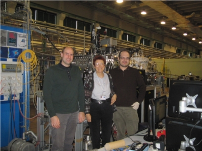
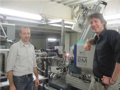
- • Dr. Anna Wolska, Dr. Marcin Klepka, and Dr. Ryszard Sobierajski – Task 2.14 European X-ray Free-Electron Laser GmbH
In the framework of task 2.14 of work package "Enhancing of human potential through exchange of know-how and twinning activities with partnering organization" Dr. Anna Wolska, Dr. Marcin Klepka and Dr. Ryszard Sobierajski from IF PAN visited the European X-ray Free Electron Laser (Eu-XFEL) facility in the period of January 24th - 27th, 2014.
The goal of the visit was to get acquainted with the measurements technique of time-resolved X-ray spectroscopy through common experiments with Dr. Wojciech Gawelda – research scientist for femtosecond X-ray experiments at Eu-XFEL. The visitors have participated in the time-resolved X-ray spectroscopy of biological samples experiment. This experimental technique provides information on the dynamics of the structural changes in samples under optical laser excitations and can be very useful for studies of the photoinduced processes in biological samples. During experiments at the at the P01 beamline at PETRA III synchrotron time-resolved changes of X-ray emission and absorption of Fe(CN)6 in water solution were studied after pumping with optical laser. The visitors got acquainted with the instrumentation, samples selection’s rules and applied measurement’s techniques. They have also learned about possible applications of the time-resolved X-ray spectroscopy technique with the X-ray free electron lasers, like Eu-XFEL. Furthermore, participants got familiarized with the scientific research performed by the FXE (Femtosecond X-ray Experiments) group at the Eu-XFEL and discussed with Dr. Wojciech Gawelda particular details concerning further collaboration in the topic of the time-resolved investigation of ultrafast processes in condensed-matter and biological systems.
|

| 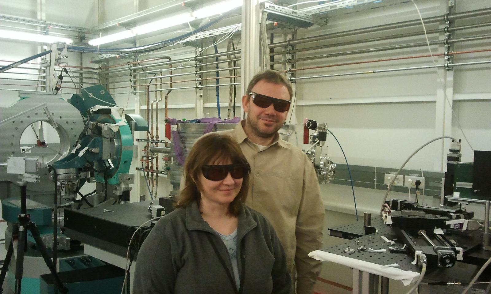
|
- • Dr. Tian Li – Visited Johannes Kepler University, Linz, Austria
In the framework of task 2.8 of work package "Enhancing of human potential through exchange of know-how and twinning activities with partnering organization" Dr. Tian Li visited Johannes Kepler University, Linz, Austria between January 12th - 26th, 2014.
The aim of the visit was specimen preparation for TEM and characterization of AlGaN:Mn samples.
A number of epitaxial (Al,Ga)N:Mn specimens have been prepared for high-resolution transmission electron microscopy (HRTEM) measurements together with reference samples not doped with magnetic ions [clean (AlGa)N]. Low- and high-resolution TEM measurements have allowed to reveal a periodic modulation of the Al-content in planes perpendicular to the growth direction (c-axis of the crystal). Preliminary measurements show that the mentioned modulation is present in samples with a nominal concentration of Al < 20%, while it is not revealed in more concentrated specimens. Furthermore, an Al modulation has been detected also in a reference (Al,Ga)N sample. Further measurements will shed light on the role of Mn-codoping, spontaneous and piezoelectric local fields and possibly strain in the formation of these superlattice-like structures with potential influence on the understanding and control of e.g. interfacial 2DEGs and 2DHGs. Details on the optimal preparation of the specimens for the dedicated HRTEM measurements of nitrides have been acquired at JKU and transferred to IF PAN, while an overview over methods for image analysis used at IF PAN has been provided to the colleagues at JKU.
During the time of the visit at JKU regular meeting with the JKU partner group have been exploited to refine the plans and strategy for the future exchange visits in the frame of the EAgLE project.
The technical knowledge acquired at JKU during this visit and the discussions with the JKU colleagues have extended the know-how in nitride samples fabrication and preparation for HRTEM measurements transferable to IF PAN. On a larger scale and in the extended perspectives of the EAgLE project – e.g. being the samples produced and investigated at JKU being studied also at the ESRF in Grenoble (EAgLE partner) – the role of IF PAN in the multidisciplinary exchange in the frame of the project has been promoted, together with the perspectives for a tighter collaboration and exchange with both JKU and ESRF.
- • Dr. Iwona Kowalik - Visit to Uppsala University, Sweden
In the framework of task 2.15 of work package "Enhancing of human potential through exchange of know-how and twinning activities with partnering organization" Dr. Iwona Kowalik visited Uppsala University, Sweden between November 29th - December 12th, 2013.
The goal of the visit at Uppsala University was to increase the expertise of the IF PAN in the area of understanding and quantitative analysis of core level spectra, an area where Uppsala provides practical expertise.
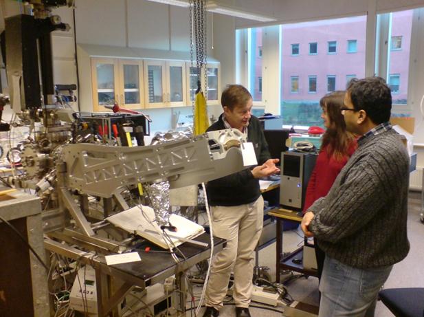 During the visit together with Uppsala researchers we discussed the procedures for the extraction of weak signals in XAS spectra, in order to increase the accuracy of the extraction of small XLMD signals. As XLMD signals are very weak and only very little information on that matter can be found in the literature, this type of analysis is challenging and important for the area of magnetic semiconductors, especially for the IF specialized in the growth of this family of materials. The analysis procedures are under development, they will be applied at IF for systematic data analysis and further developed in the future in collaboration with researchers from Uppsala University.
It was also discussed the modelling and analysis of ZnO spectra using the FEFF code with the expert working in the absorption spectroscopy field. The first attempts for O K-edge modelling shows that FEFF is the correct tool for these type of simulations. Also, some practical details were discussed for resonant inelastic X-ray scattering core level spectroscopy at MAX-lab.
With the Uppsala senior staff, future visits at IF PAN of two professors from the Department of Physics and Astronomy at Uppsala University were discussed. Prof. Rajeev Ahuja, a theorist in the area of magnetism and Prof. Jan-Erik Rubensson, an experimentalist and expert in RIXS spectroscopy, responsible for the development of the new VERITAS beamline at the synchrotron radiation facility MAX VI in Sweden could visit the IF PAN in 2014.
The visit increased the research potential of IF PAN in the area of data analysis of L-edge core level spectra. For XAS spectra taken with linear light it was found possible to extract the small linear dichroism contribution. Various technical details were discussed on the design of the RIXS end stations at MAX IV, to allow for magnetism related RIXS experiments, on typical magnetic semiconductor samples grown at IF PAN, at the VERITAS beam line of MAX IV.
- • Dr. Ryszard Sobierajski – Task 2.14 Tutorial course on the XFEL optics wavefront propagation simulations
In the framework of the task task 2.14 within the work package "Enhancing of human potential through exchange of know-how and twinning activities with partnering organization" Dr. Ryszard Sobierajski from IF PAN attended between November 27th and 29th, 2013 a tutorial course on the XFEL optics wavefront propagation simulations organized by Dr. Liubov Samoylova from European XFEL. The course started with a general introduction to the PYTHON software. Next the SRW (Synchrotron Radiation Workshop) and WPG (WaveProperGator) software packages were presented. They are used to perform simulations of the wavefront propagation, in particular coherent X-ray radiation. Finally application examples of general interest, including simulations of the wavefront propagation through CRLs, offset and KB mirrors were discussed. An example of the calculated intensity distribution behind an imperfect X-ray mirror is presented on a figure below.
|
|
The SRW and WPG software packages are important tools required for design of optics and experimental stations for the short-wavelength free electron lasers like European XFEL. It is planned to use these tools within the collaboration with FXE (Femtosecond X-ray Experiments) instrument group at European XFEL to evaluate the influence of optics on the intensity distribution in the focal point at FXE beam line. This can be a base to establish a further collaboration in the topic of the time-resolved investigation of ultrafast processes in condensed-matter systems.
Moreover a meeting with Dr. Harald Sinn (leader of the X-ray Optics & Beam Transport group) and Dr. Andrew Aquila (Research scientist for coherent X-ray imaging) from European XFEL was carried out in order to discuss particular details concerning our future collaboration. The tight cooperation between the two centers will have a significant impact on increasing of IF PAN workers' skills in the field of experimental techniques used at X-ray free electron lasers. Such collaboration will also have a positive impact on the integration of IF PAN researchers in the international free electron lasers users community.
|
- • Dr. Jarosław Domagała – Task 2.2 European Synchrotron Radiation Facility
In the framework of task 2.2 of work package "Enhancing of human potential through exchange of know-how and twinning activities with partnering organization" Dr. Jarosław Domagała on November 5th - 23th 2013 visited the EAgLE scientific partner, European Synchrotron Radiation Facility, located in Grenoble, France.
During his stay Dr. J. Domagała visited three experimental stations: BM05 - “X-ray Imaging and Optics Beamline”, ID01 - Microdiffraction Imaging Beamline, Nanodiffraction, coherent diffraction, anomalous SAXS (Tobias Shulli - Scientist in charge) and ID13 - Microfocus Beamline, Microfocus and nanofocus endstations - (Manfred Burghammer - Scientist in charge).
At the beamline BM05 he was involved both in experiment and initial data processing in the investigation of the defect structure of diamond plates by topographic method with strain resolution up to 10-8 which is 3 orders of resolution better than what can be obtained in a standard laboratory conditions. At the beamline ID01 he had the opportunity to follow the process of collecting diffraction signal from separated nanoobject. Dr. Domagała was involved in sample alignment procedure, data collecting, initial data processing and in the process of beam energy changing and monochromators adjustment.
At the ID13 beamline Dr. Emanuela Di Cola introduced him to two different experimental hatches and specified problems and materials investigated there. Dr. Domagała got some experience with the software environment necessary to manipulate samples and different detectors during measurements. He was also introduced to the graphic software for data visualization.
|
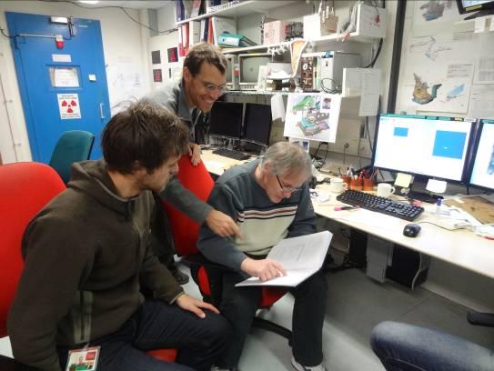
| 
|
ID01 : (from right) Joel Eymery, Tobias Schulli (ESRF scientist), Ondrej Matula
| ID13: Emanuela Di Cola (ESRF scientist)
|
- • Dr. hab. Sławomir Kret – Visited University of Warwick, United Kingdom
In the framework of task 2.3 of work package "Enhancing of human potential through exchange of know-how and twinning activities with partnering organization" Dr. hab. Sławomir Kret on October 20th - 26th 2013 visited the EAgLE scientific partner Department of Physics, University of Warwick, United Kingdom.
During stay Dr. hab. Sławomir Kret visited the Facilities of Physics The Electron Microscopy laboratory within the Physics Department and obtained information about detail specification and research possibilities of WoU’s transmission electron microscopes facilities. During this stay, Dr. Kret gave two talks: on “EAgLE project at institute of physics Polish Academy of Science“ and “History and present research at Electron Microscopy Group of Institute of Physics Polish Academy of Science“. Given at UoW presentations permitted us to disseminate information about EAgLE project and research of electron group of IF PAN at the UoW, which resulted in identification the range of research topics interesting for both groups.
|
| 
|
Building of department of Physics of University of Warwick , TEM/SEM facilities and EAgLE project presentation.
|
Dr. Kret also meet with Professor Chris McConville. They discussed about possibilities of adding as a subject of common research structural problems related to complex oxides layers (LaAlO3, LaNiO3, SrTiO3, LaMnO3) prepared by Pulsed Laser Deposition techniques. During meeting with with PhD student Adam Dyson Dr. Kret discussed the possibility of collaboration in domain of automation of TEM experiment by developing of scripts and plugins to existing software of microscopes.
|
- • Prof. Dr. hab. Krystyna Jabłońska, Dr. Iraida N. Demchenko – Task 2.4 - Meetings with the leaders of ALBA synchrotron
In the framework of task 2.4 of work package "Enhancing of human potential through exchange of know-how and twinning activities with partnering organization" a series of meetings with the leaders of ALBA synchrotron were carried out in order to discuss particular details concerning our future collaboration. Namely, we were able to meet the Ramon Pascual - Chairman of ALBA Synchrotron Executive Board and President of the Royal Academy of Sciences and Arts of Spain, Caterina Biscari - the director of the Laboratory of Synchrotron Light CELLS - ALBA; Gaston Garcia - Deputy Director; Miguel Aranda - ALBA's Scientific Director; Alejandro Sánchez - ALBA's Responsible Officer for the EU projects and contacts with industry; Eric Pellegrin - Soft X-ray beamlines supervisor; beamline scientists or/and staff of BL04 - MSPD: Materials Science and Powder Diffraction, BL09 - MISTRAL: X-ray Microscopy, BL22 - CLÆSS: Core Level Absorption & Emission Spectroscopies, BL24 - CIRCE: Photoemission Spectroscopy and Microscopy, BL29 - BOREAS: Resonant Absorption and Scattering. During these meetings it was possible to familiarize with ALBA's features and future plans. A few propositions concerning collaboration between IF PAN and ALBA under EAgLE project were made and discussed. One of the central issues of the meeting with ALBA's Scientific Director was scheduling of twinnings between our centres with special emphasis on establishing of long term cooperation with ALBA synchrotron. Several corrections of working schedule were suggested by M. Aranda taking into account the technical development of beamlines of interest. Further, the proposals of activities foreseeing in EAgLE project which may be interested for ALBA's scientists and particular postdocts were tendered and discussed. The tight cooperation between the two centers will have a significant impact on increasing of IF PAN workers' skills in the field of characterization of modern materials by using a variety of synchrotron techniques. Such collaboration will also have a positive impact on the integration of IF PAN researchers in international cooperation.
- • Dr. Maciej Zgirski – Visited Aalto University, Espoo, Finland
In the framework of task 2.9 of work package "Enhancing of human potential through exchange of know-how and twinning activities with partnering organization" Dr. Maciej Zgirski visited Lounasma Laboratory, Aalto University, Espoo, Finland between June 30th - July 5th, 2013.
The aim of the visit of Dr. Zgirski was to get familiar with dry dilution fridges and agree on further collaboration within project.
Discussions with main lab engineer Dr. Aleksander Savin on the issues related to purchase of a dilution refrigerator were carried out. Dr. Savin is in charge of 16 dilution refrigerators and his experience in the subject is extraordinary. He spotted out weak and strong points of designs available on the market. A few BlueFors systems was shown to me during on-site inspection. BlueFors company will be seriously considered in the public procurement procedure. I am leader of the Task 4.3 and 4.4 (purchase of dilution refrigerator). Hence his help is very valuable for me. We discussed wiring of the cryostat (cables, filters, thermometers), an optimal installation of a dilution refrigerator (e.g. how to remove mechanical vibrations).
Finally, the main values of this visit are: the acquiring of the vital information on drawbacks of cryogen-free dilution refrigerators, and on comparison between the "dry" cryogenic systems with traditional "wet" systems; consultations on wiring, filtering, and thermalization procedures for the new dilution system which lead to a substantial enhancement of our cryogenic expertise. The obtained information will be crucial for the process of selection of the new dilution refrigerator for IF PAN.


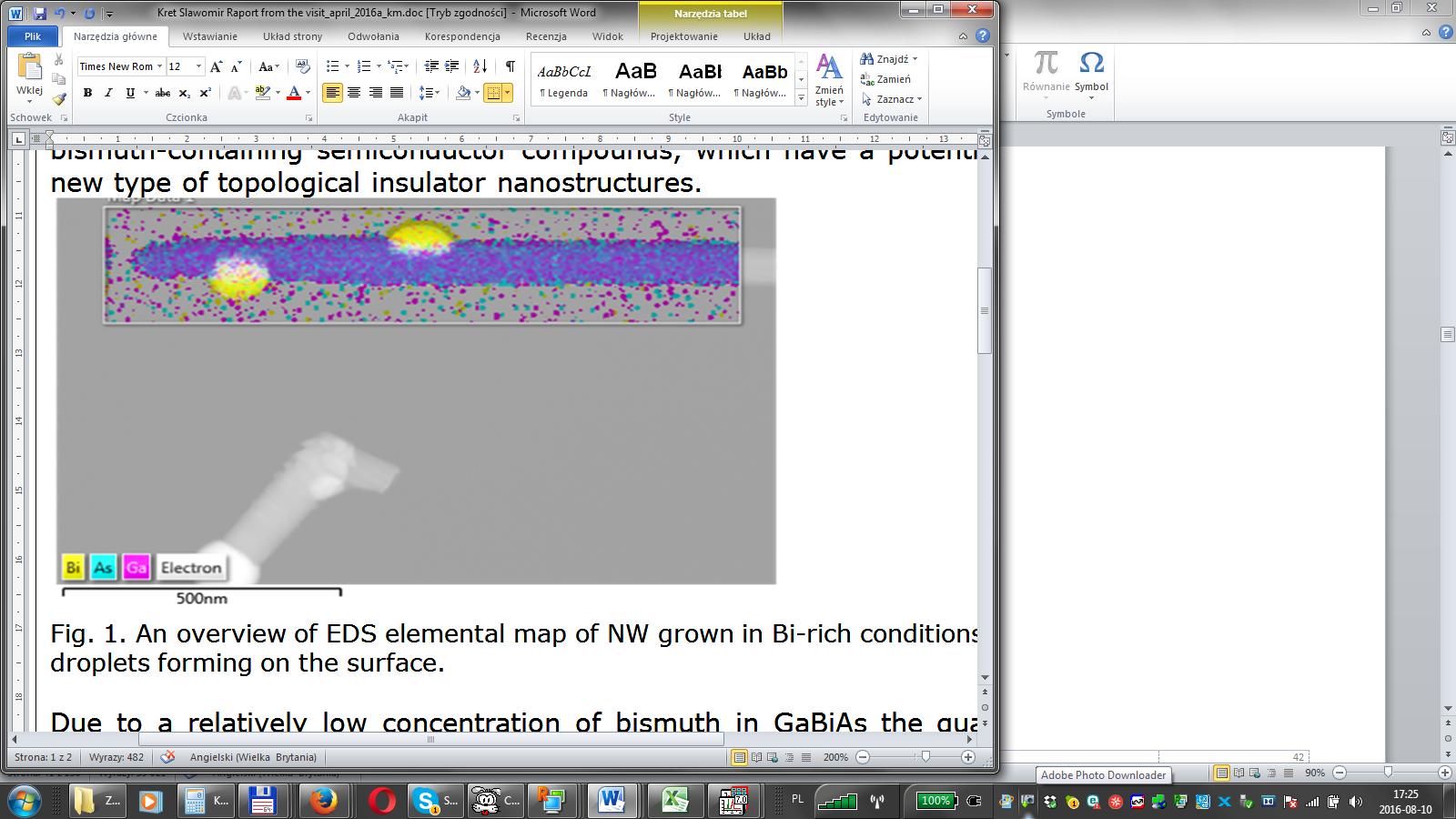
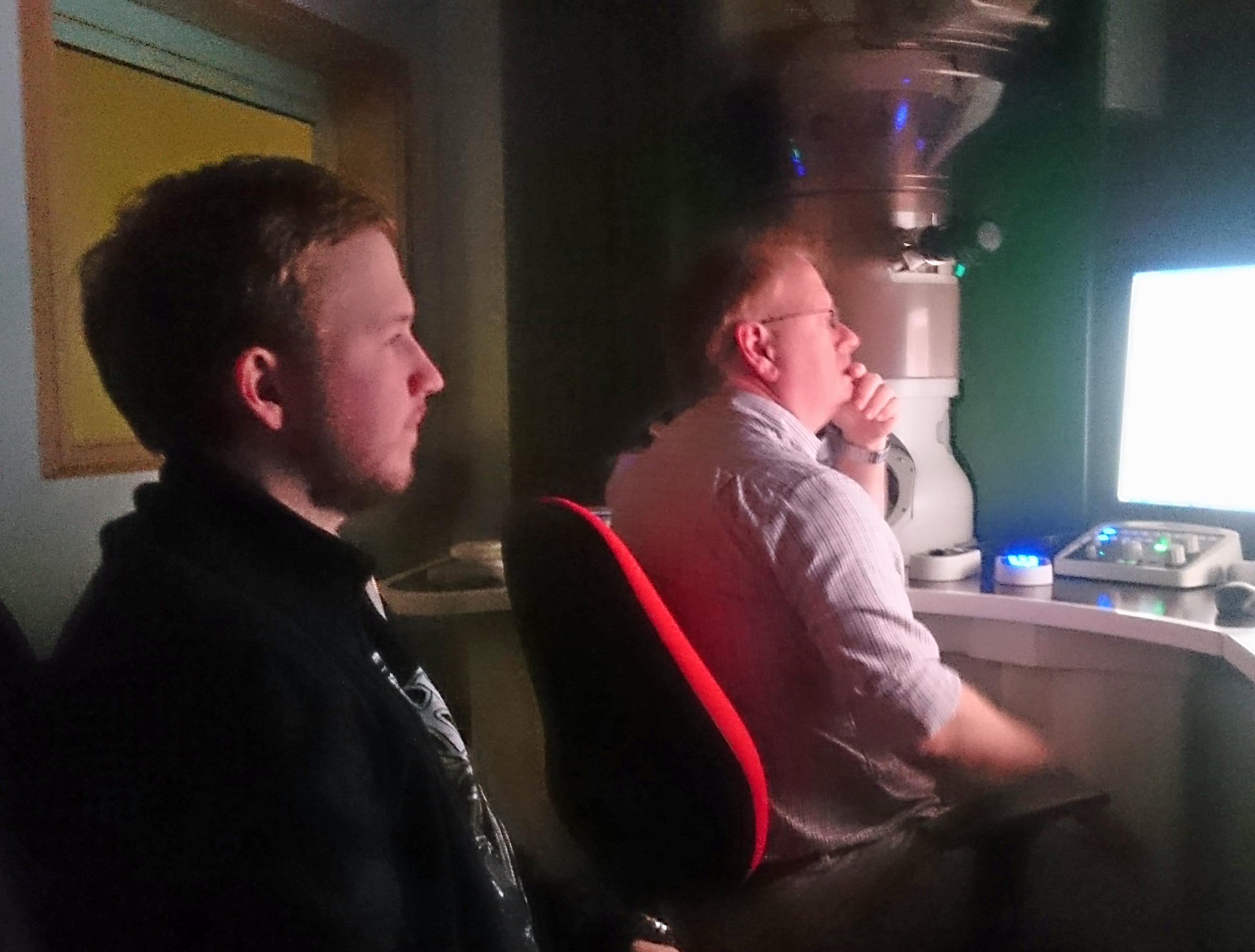
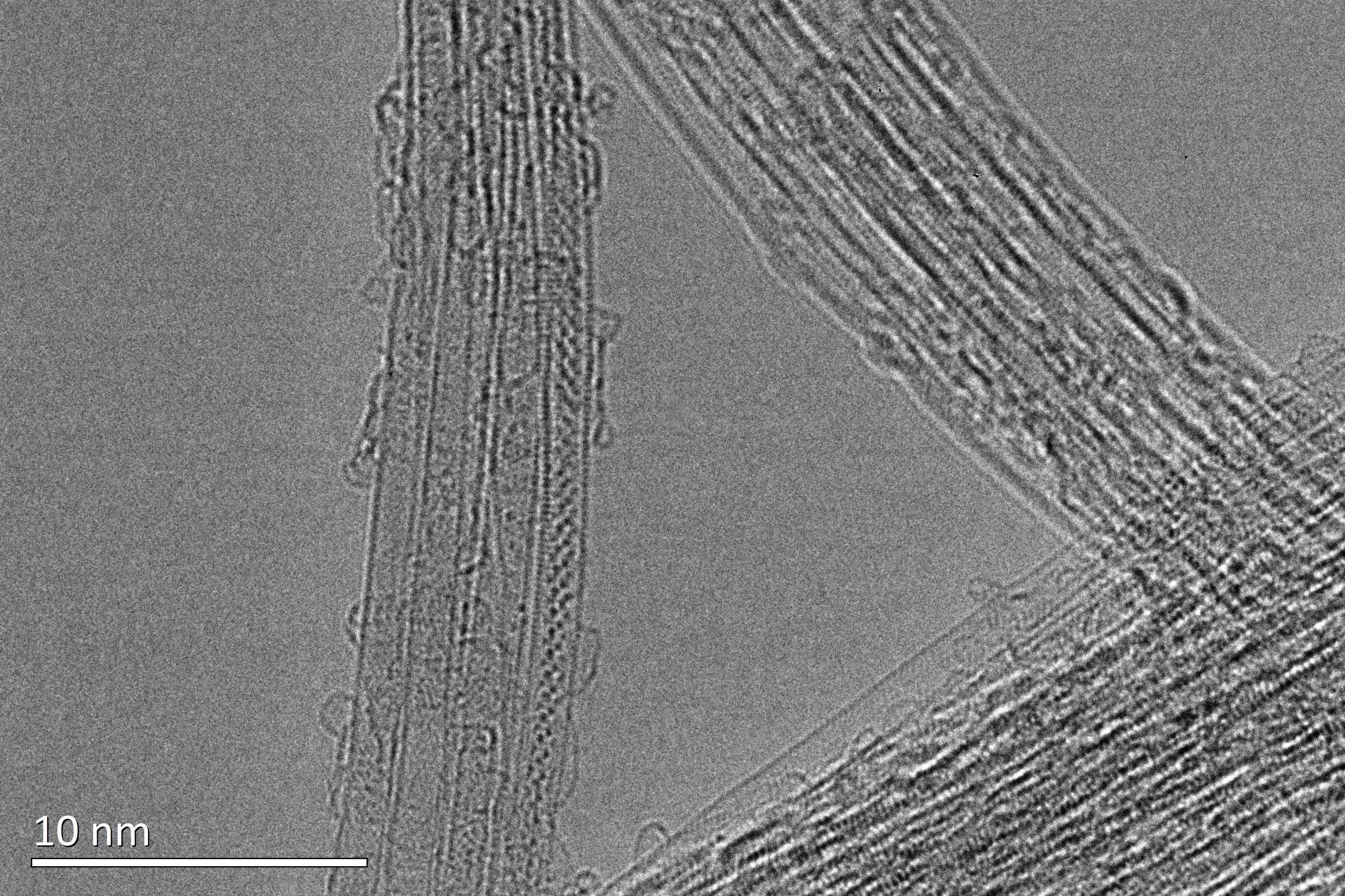
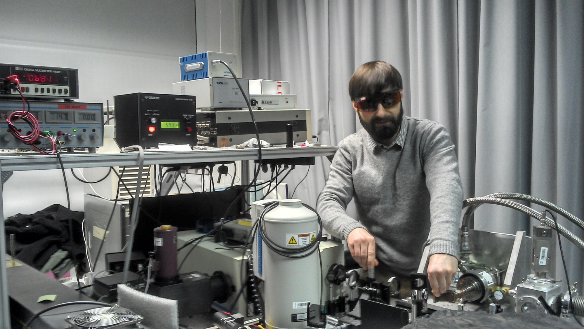
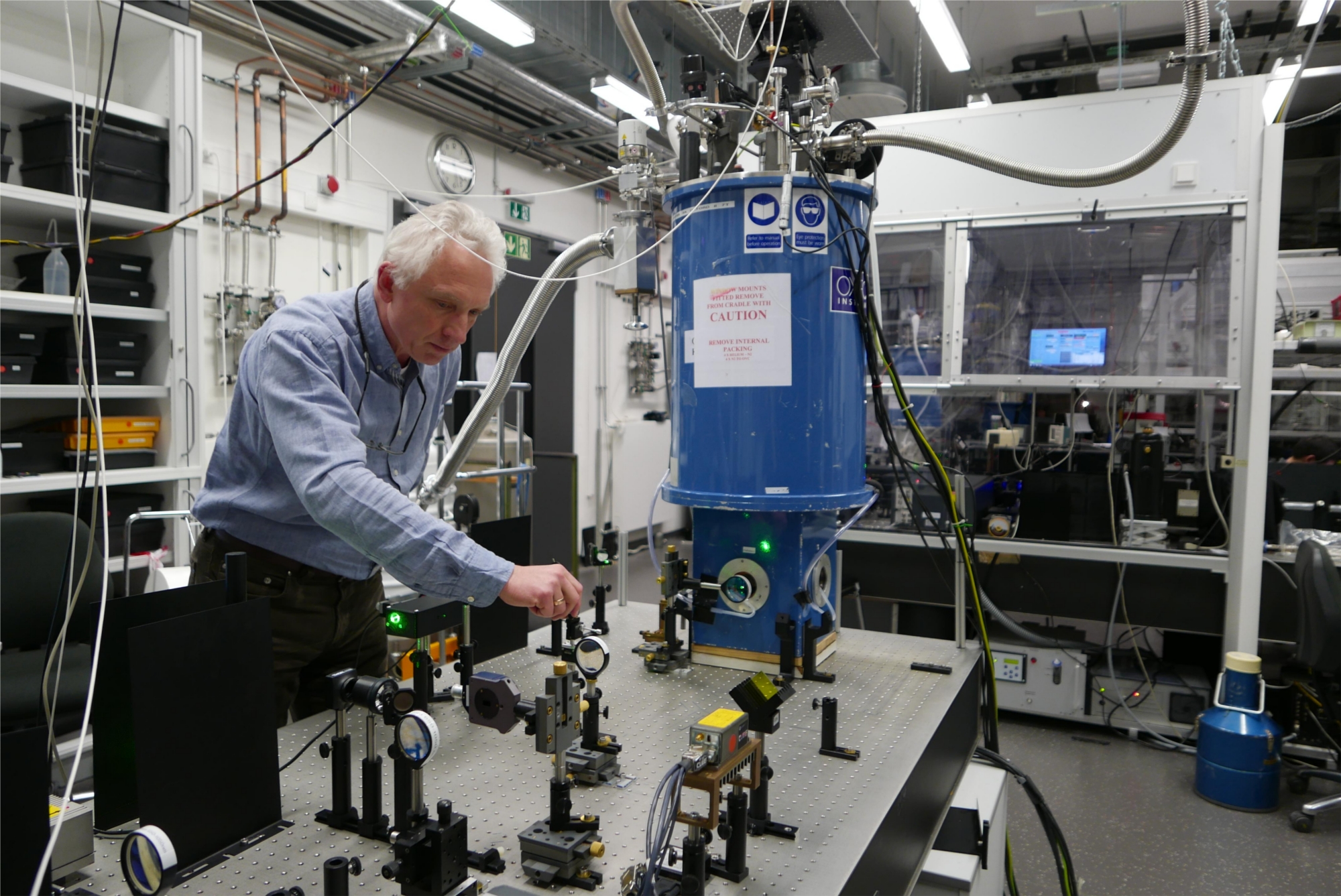

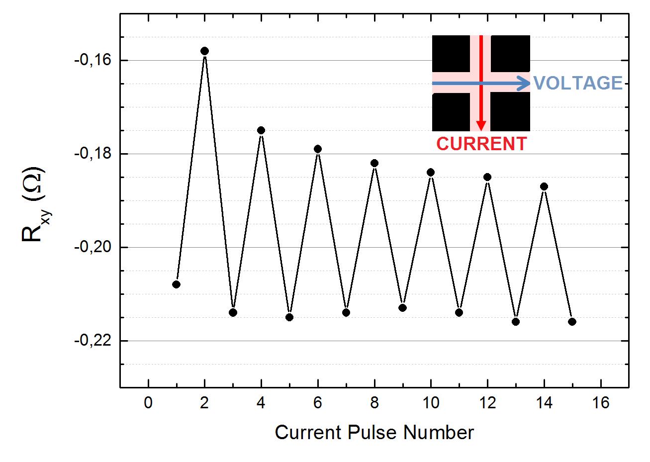
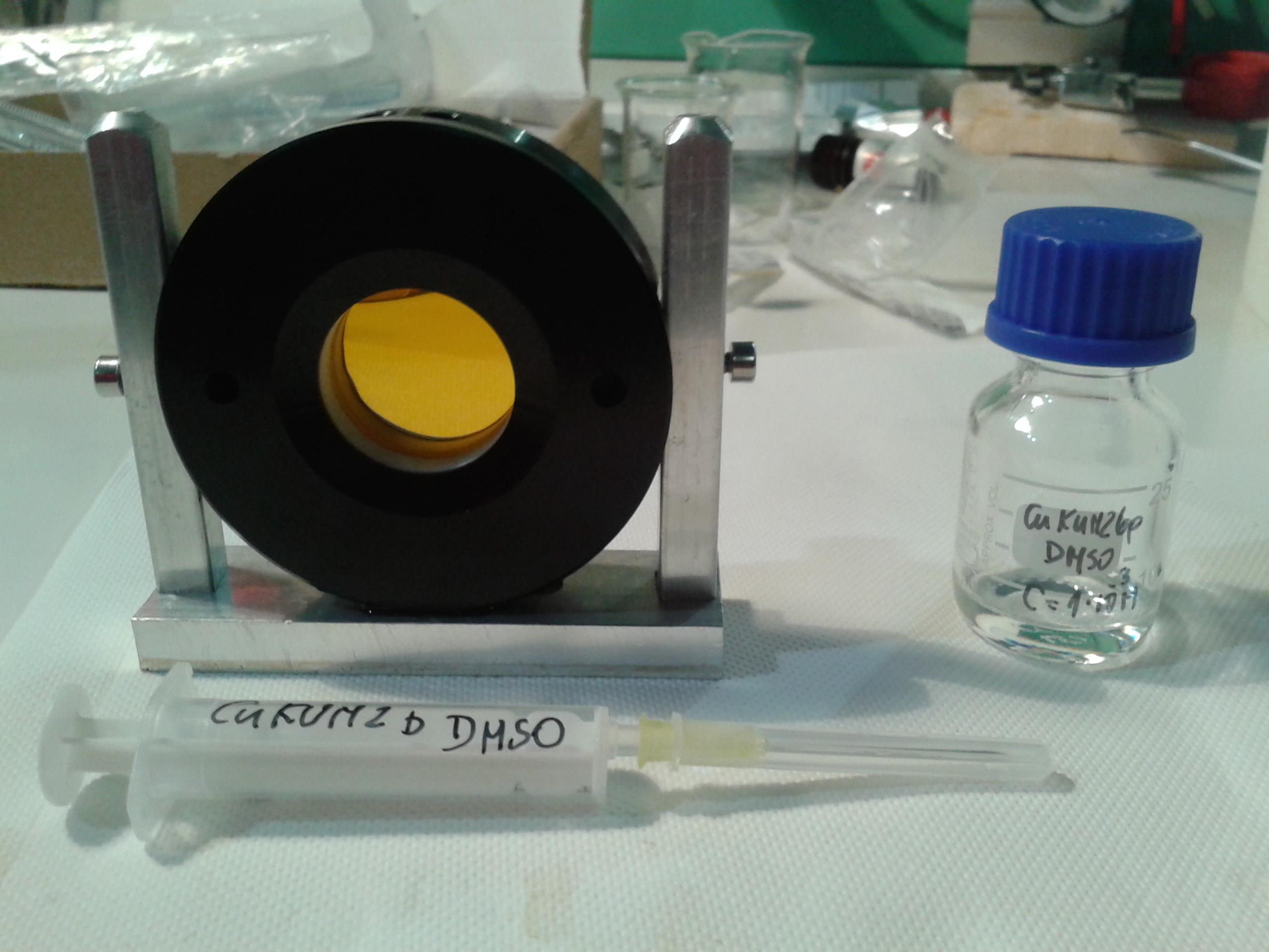

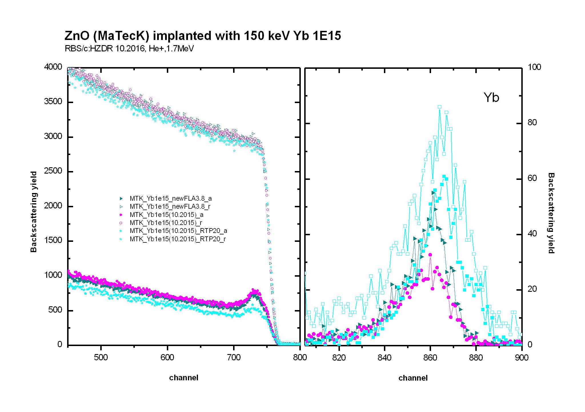


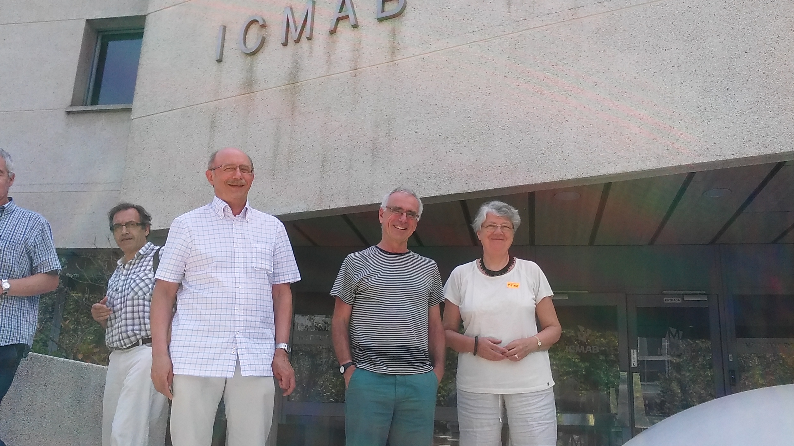

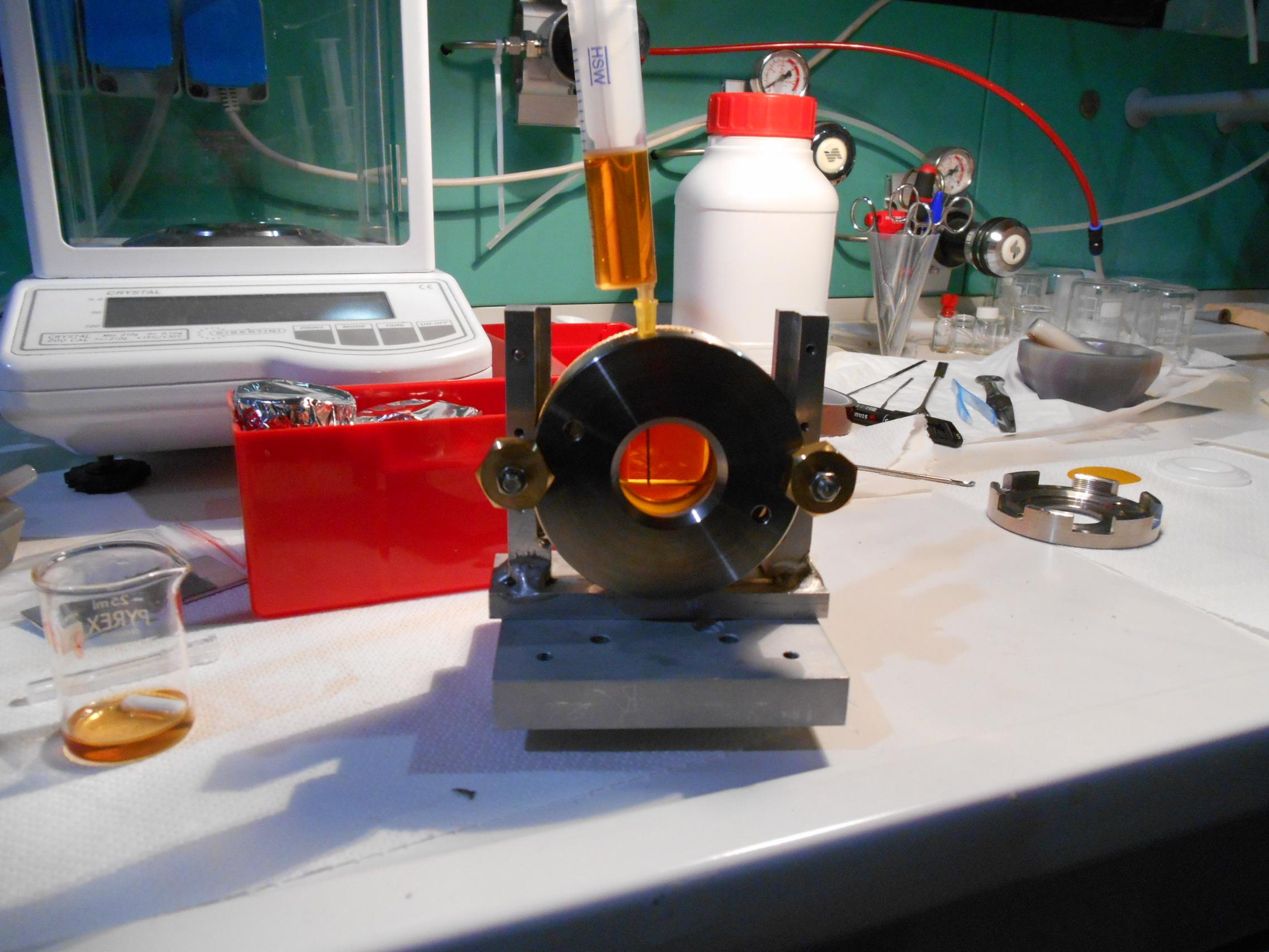

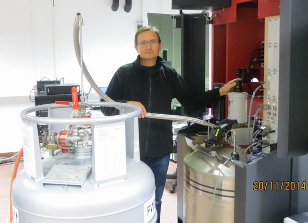
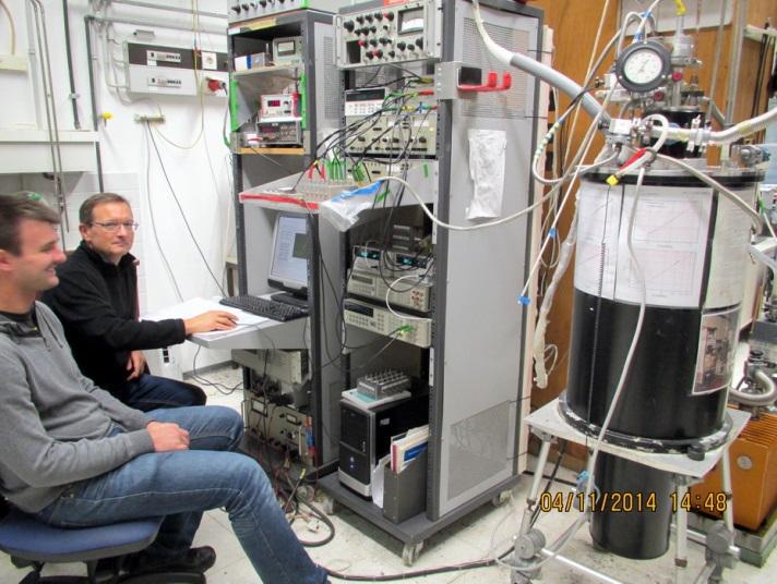

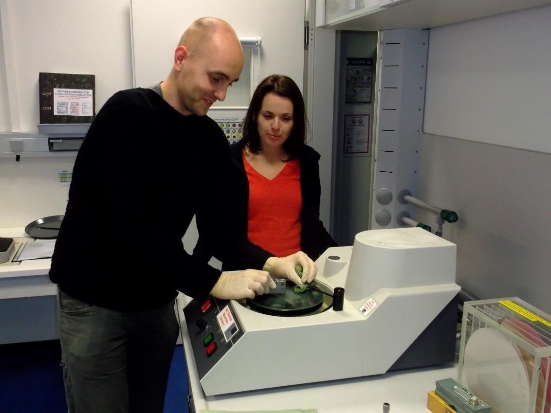
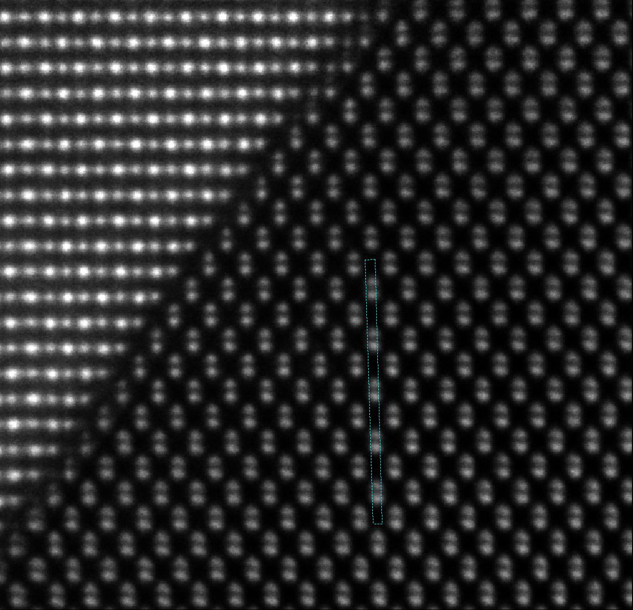


