Characterization - Scanning Electron Microscopy (SEM)

Scanning Electron Microscopy (SEM)
|
DescriptionThe ultra-high resolution scanning electron microscope Hitachi SU-70 (image resolution ~ 1 nm) is suitable for investigations of morphology and properties of solids, in particular semiconductors (including wide-gap systems) and semi-insulating materials. It is equipped with two secondary electron (SE) detectors and one back-scattered electron (BSE) detector. The latter enables high-sensitivity imaging with atomic and density contrast. The microscope is also fitted with the X-ray microanalysis system (EDX) and the cathodoluminescence spectrometer GATAN Mono CL3. With such multipurpose equipment the microscope is particularly suitable for comprehensive studies of correlations between microstructure, chemical composition and optical properties of complex systems. Parameters- Shottky-type field-emission electron gun
- Two secondary electron (SE) detectors: upper (“in lens”) and lower, emphasizing the surface topography
- Semiconductor back-scattered electron (BSE) detector for imaging with atomic and density contrast
- Transmitted electron detector enabling scanning transmission electron microscopy (STEM) in bright- and dark-field modes
- Acceleration voltages (AV): 0.5-30 keV
- Electron beam current: picoampers for imaging, nanoampers for analytical applications
- Maximum sample diameter: 5 inches
- Nominal image resolution: 0.8 nm
- X-ray microanalysis system
- cathodoluminescence system for high resolution imaging and spectroscopy GATAN Mono CL3
|
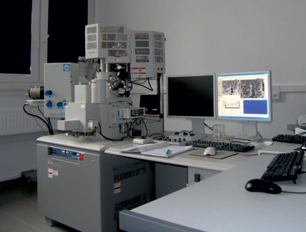
Scanning electron Microscope Hitachi SU-70. |
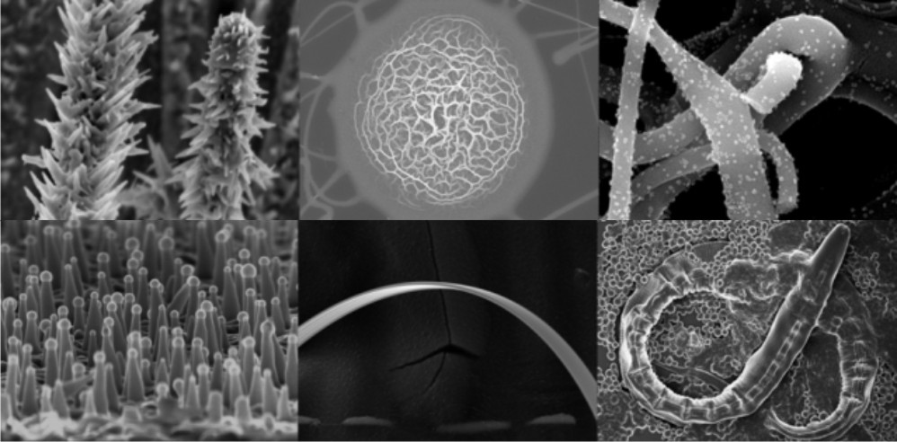
Sample surface SEM images. |
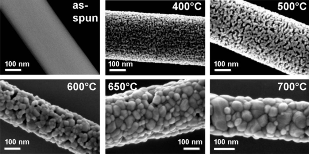
Sample SEM images of ZnO nanofiber after series of annealing processes. |
|