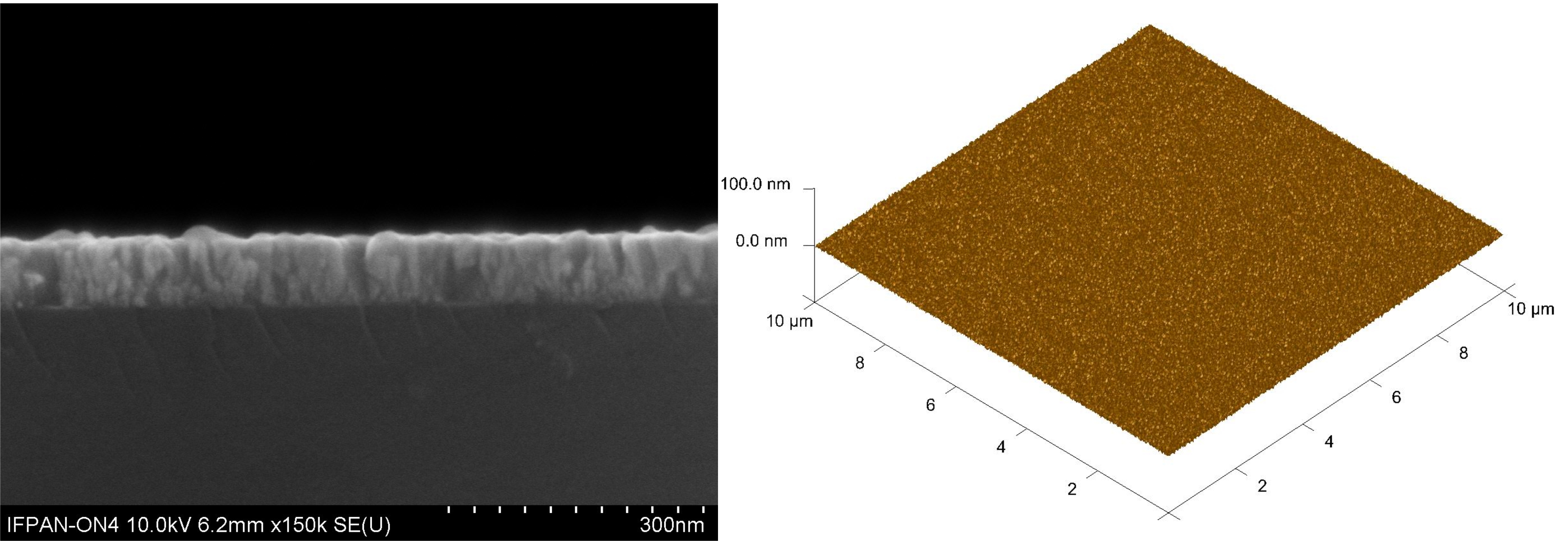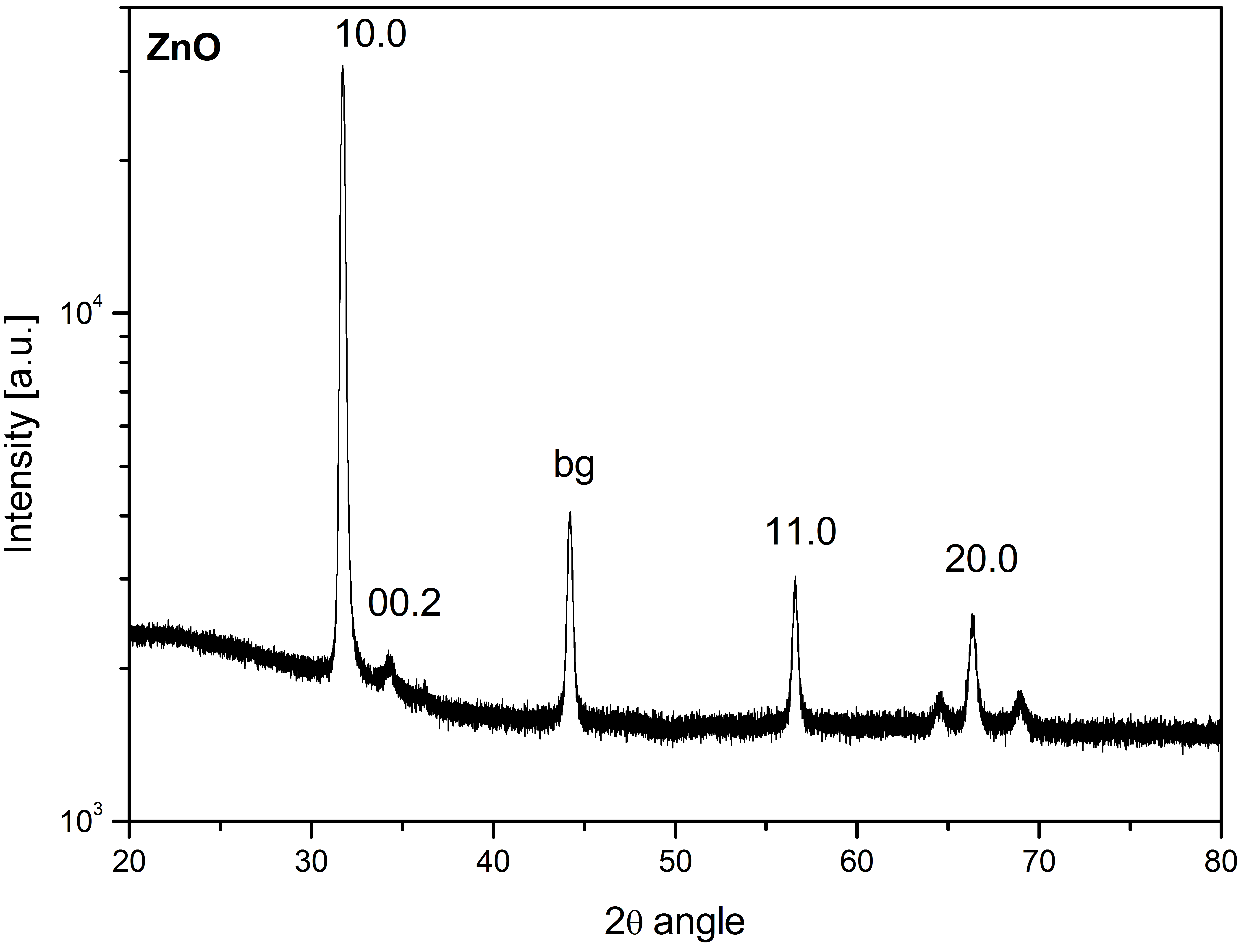

Policrystalline layer of zinc oxide | ||||
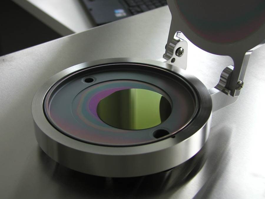
DescriptionZinc oxide (ZnO) thin films are obtained by atomic layer deposition (ALD) on many substrates, like Si, GaN, SiC, Al2O3 SiO2 etc. The material is formed in a double exchange chemical reaction between two reactants (precursors), such as a deionized water (oxygen precursor) and a diethylzinc - DEZ (zinc precursor). The use of a ammonia water (NH3۰H2O) instead of deionized water as a oxide precursor in a growth process increases the electrical resistance of zinc oxide layers. ZnO can be grown at the temperature range from 25°C to 300°C. The maximum size of the substrate is 20 cm of a diameter.
Specification
ApplicationsZnO is semiconductor material, which is investigated for many possible applications in electronics, optoelectronics and photovoltaics. Physical and chemical properties of ZnO give us a great possibility of use of this material in devices, such as display panels, light emitting diodes or solar cells. Due to a wide band gap, ZnO is a transparent material in the visible range, so it can successfully be used in the so-called. "transparent electronics." Simultaneously, ZnO has a very high sensitivity and thermal stability, which makes it suitable for applications in sensor devices.
|
| |||