
Titanium dioxide layers | ||||
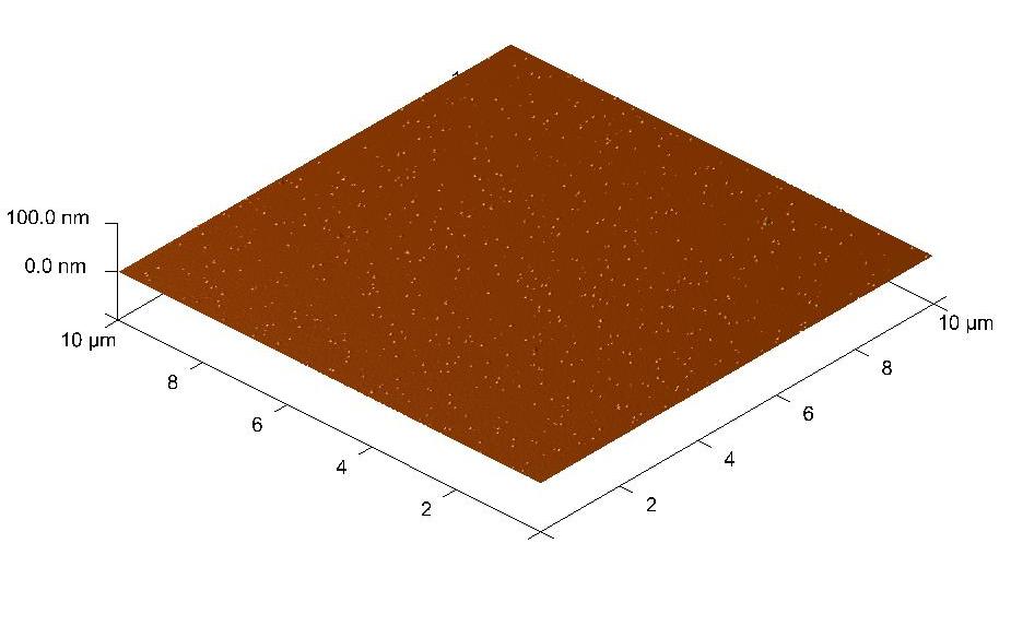
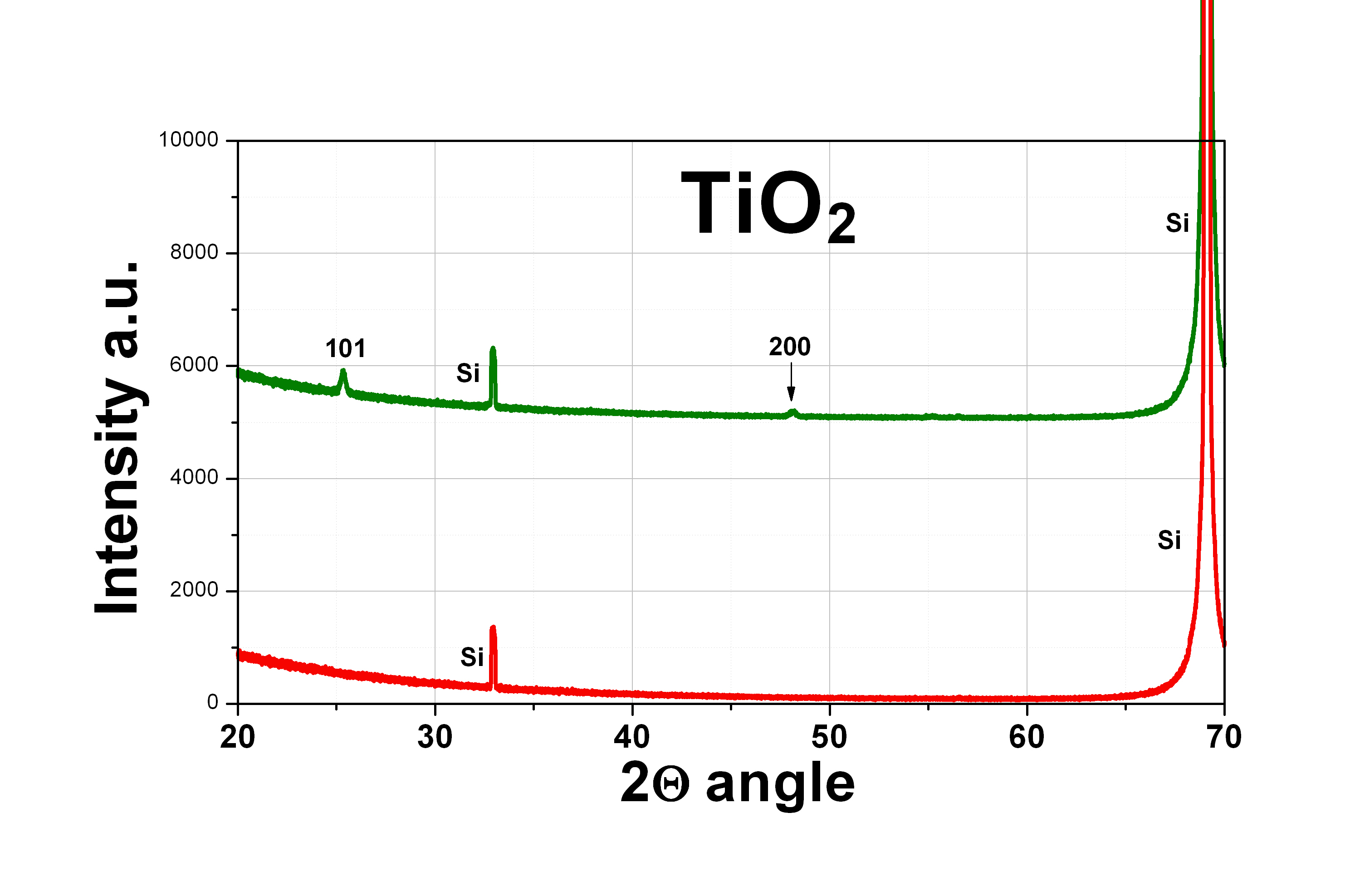
DescriptionTitanium dioxide also known as titania (TiO2) thin flims are obtained by atomic layer deposition (ALD) on range of substrates, like Si, GaN, SiC, graphene, SiO2 etc. The material is formed in a double exchange chemical reaction between two reactants (precursors), such as a deionized water (oxygen precursor) and a titanium chloride - TiCl4 or tetrakis(dimetylamido)titanium(IV) - TDMAT (titanium precursor). TiO2 can be grown at the temperature range from 25°C to 450°C. The maximum size of the substrate is 20 cm of a diameter.
Specification
ApplicationsTiO2 is characterized by high refractive index, good stability, high chemical resistance, high hardness and high permittivity. This material, due to its physical and chemical properties, can be used as an insulator in electronic devices, as optical coatings in lasers and microscopes, as well as, barrier or protective layers in photovoltaic structures. Moreover, this material can be used in various types of sensors, and can be used in the manufacture of dental prostheses and implants in medicine. |
| |||