
Hafnium dioxide layers | ||||
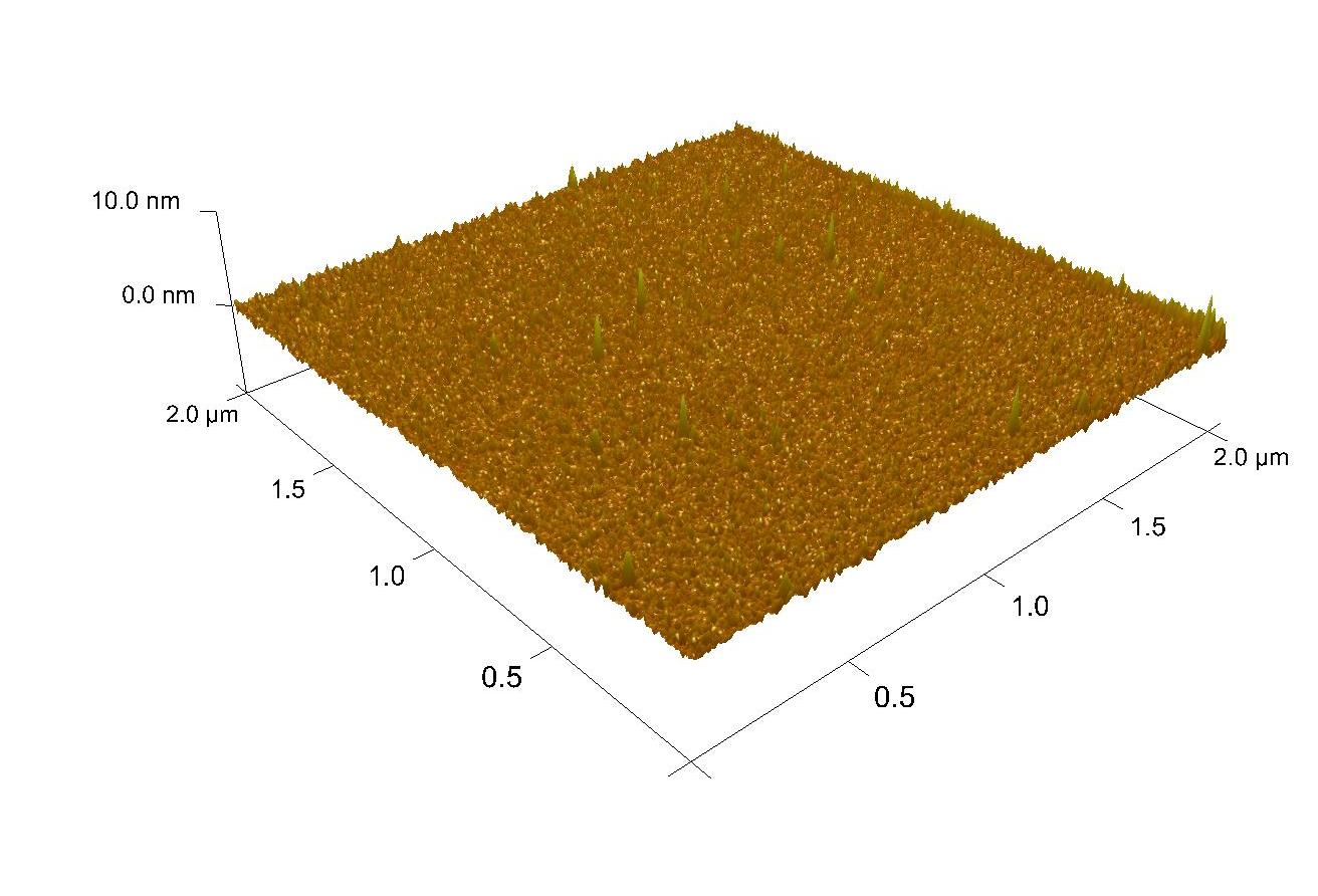
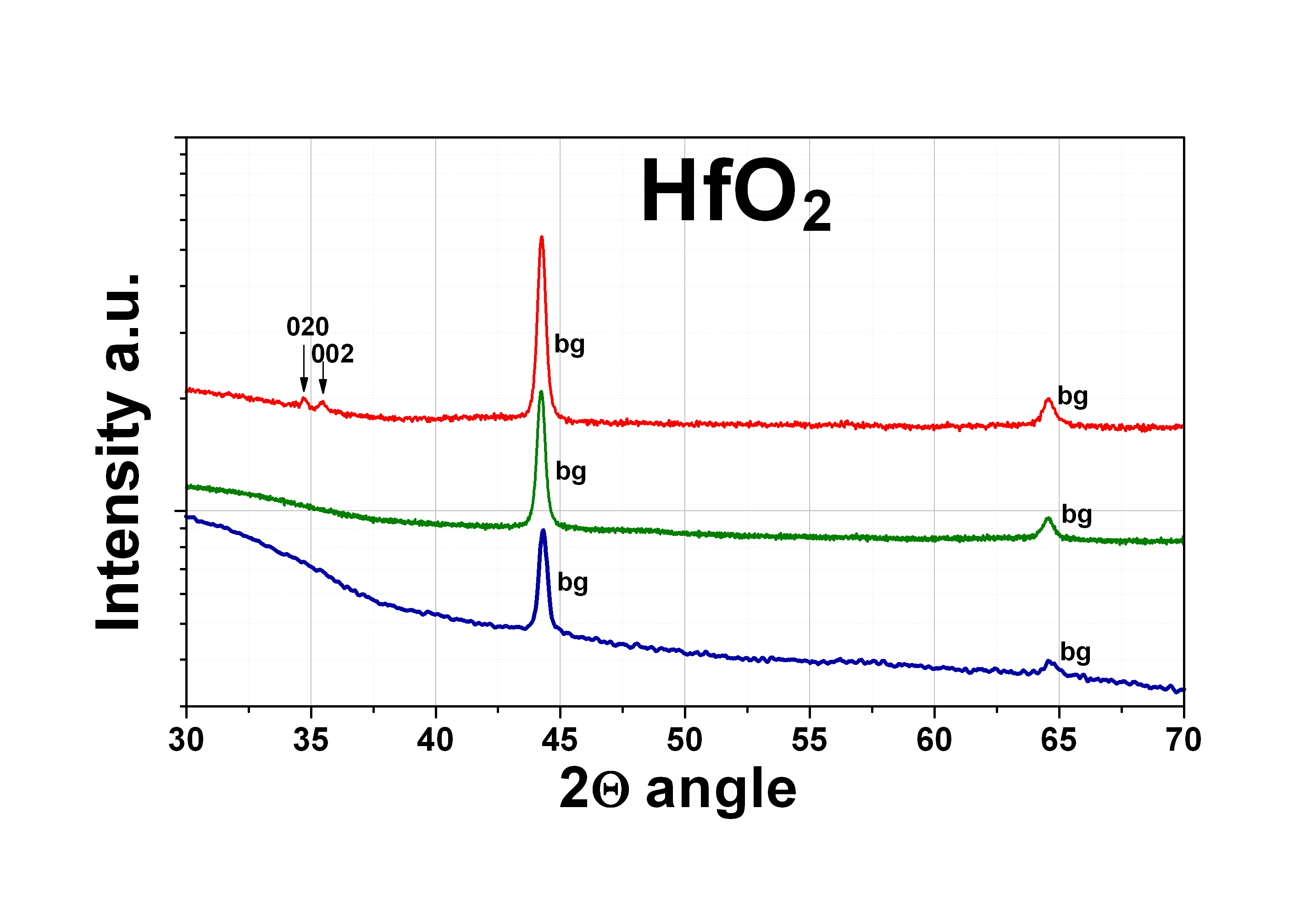
DescriptionHafnium dioxide (HfO2), also known as hafnia, thin films are obtained by atomic layer deposition (ALD) on range of substrates, like Si, GaN, SiC, graphene, SiO2 etc. The material is formed in a double exchange chemical reaction between two reactants (precursors), such as a deionized water (oxygen precursor) and a tetrakis(dimetylamido)hafnium(IV) - TDMAH (hafnium precursor). HfO2 can be grown at the temperature range from 70°C to 300°C. The maximum size of the substrate is 20 cm of a diameter.
Specification
ApplicationsHfO2 is characterized by good optical, electrical and structural properties, therefore this material can be used as an insulator in electronic devices especially in "transparent electronics", as a variable resistance material in electronic memories, as optical coatings with high refractive indices in lasers and microscopes and as a protective or barrier layers of photovoltaic structures. In addition, this material can be used in medicine and dentistry for the manufacture of prostheses and implants. |
| |||