
Amorphous insulating layers | |||
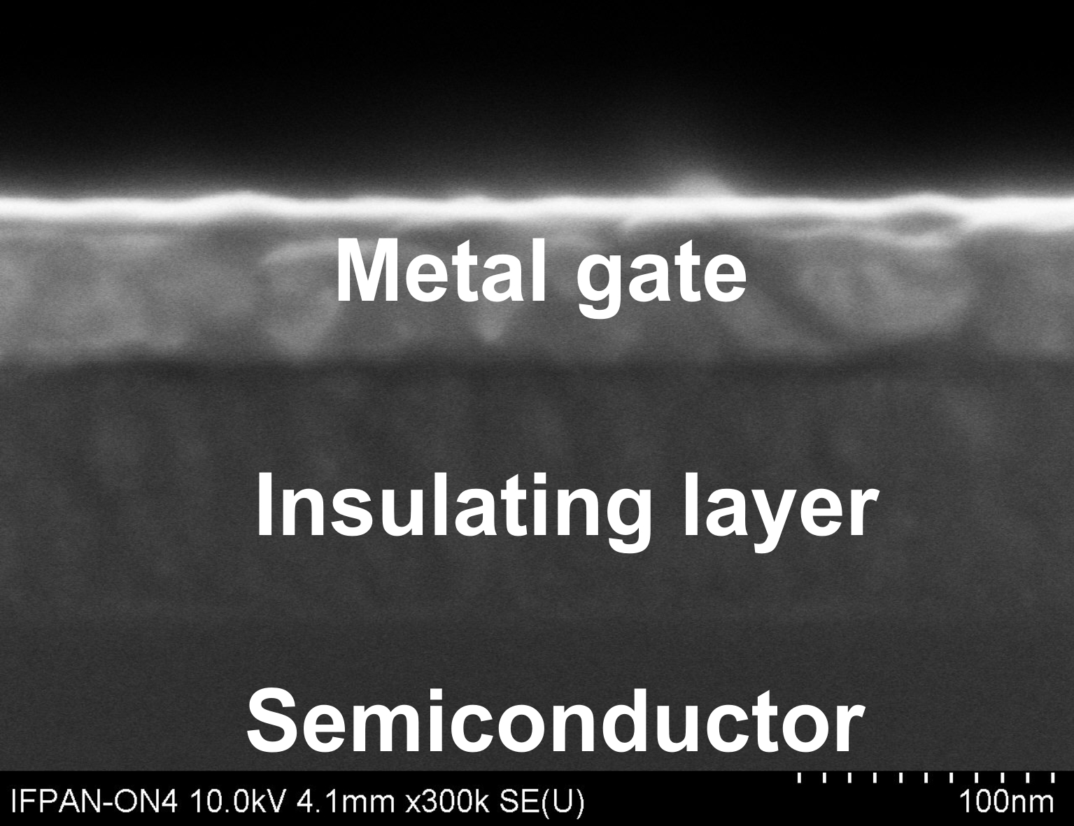
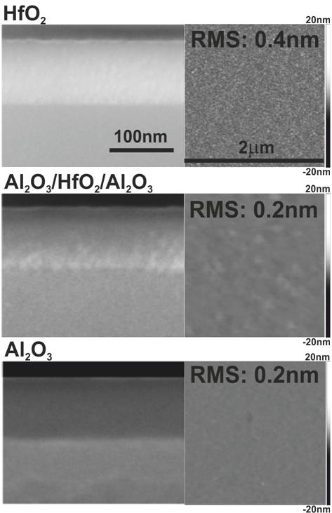
DescriptionInsulating thin films are obtained by atomic layer deposition (ALD) on different substrates: like Si, GaN, SiC, graphene, ZnO. Materials are formed in a double exchange chemical reaction between two reactants (precursors), such as an oxygen precursor and a metal precursor. Insulating layers can consist of one or more oxide materials. The compounds can be grown at low temperatures, usually below 100°C. The maximum size of the substrate is 20 cm of a diameter.
Specification
ApplicationsDeposition of dielectric layers at a low temperature, below 100 ˚ C enables the construction of electronic devices containing insulators in the interaction with different semiconductor materials such as Si, GaAs, ZnO, SiC, GaN, GaMnAs or graphene . Our studies show that the most efficient insulator is a composite layer. The combination of low temperature manufacturing and transparency of oxide layers causes that electronic devices with these materials, grown by the ALD technique, are a solid, viable, safe for the environment, and a very promising proposal for the next generation of transparent and flexible electronics.
Patent: PL395639 (13-07- 2011) |
| ||