Technological services - Physical vapor deposition (PVD)

Physical vapor deposition (PVD) | ||||
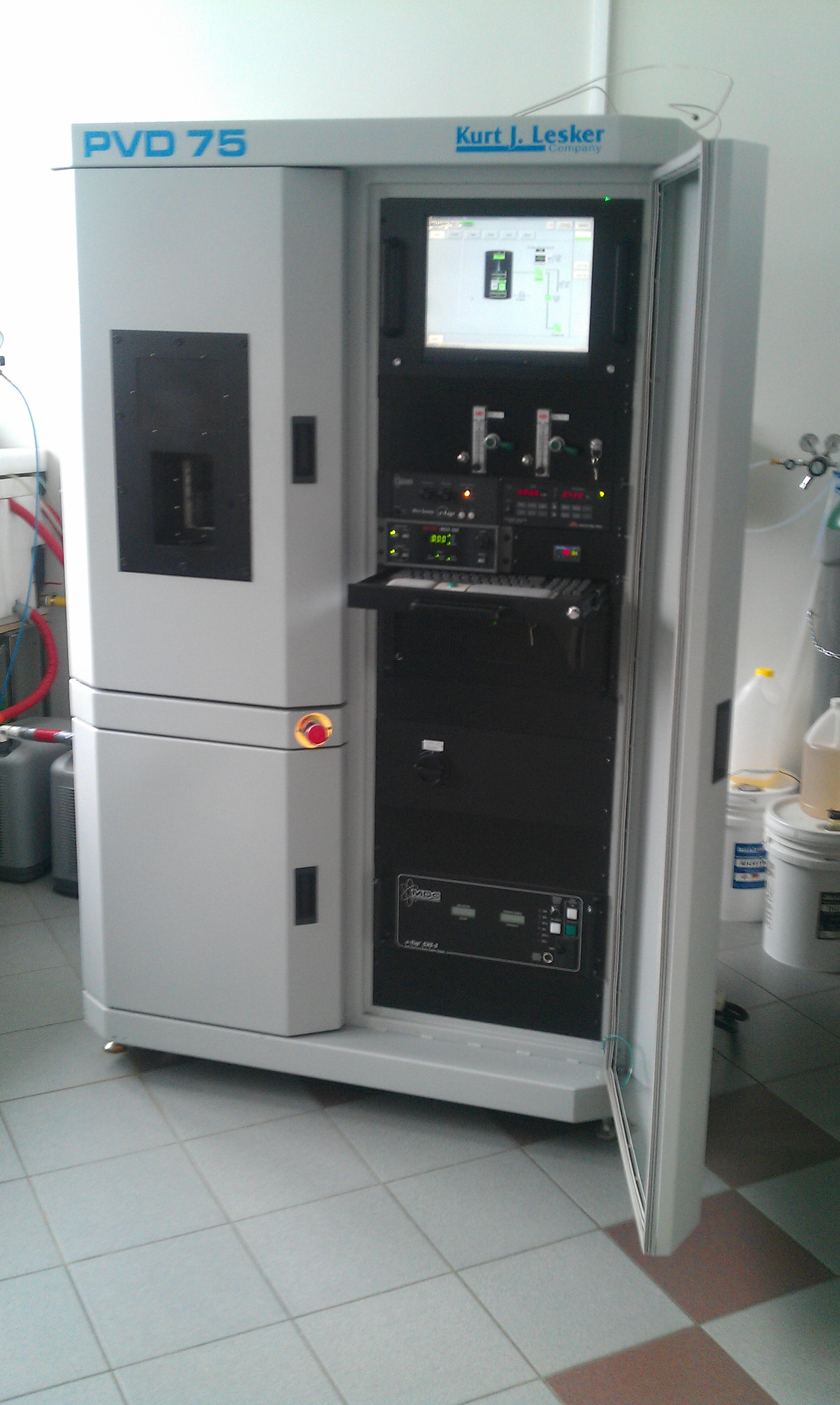
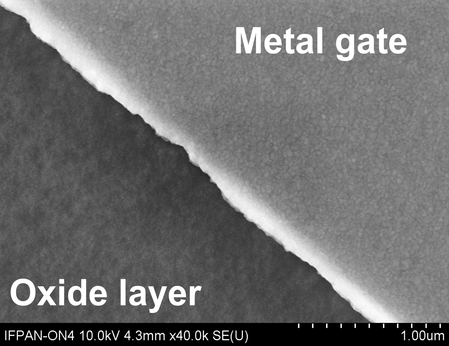
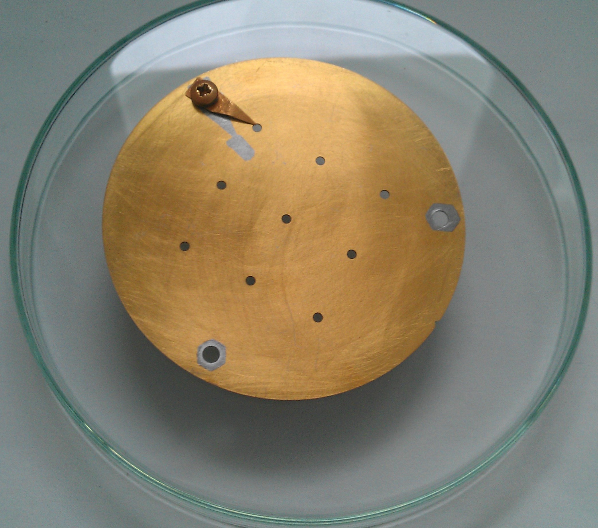
DescriptionPhysical vapor deposition (PVD) is a deposition technique of thin films from the vapor phase with use of physical phenomena, such as magnetron sputtering or cathodic sputtering. Growth process proceeds in a high vacuum system. Deposited materials crystallize on the substrate surface.
Specification
ApplicationsEvaporation of metal contacts like Au, Ni, Pt, Ag, Ti, etc. for electronic, optoelectronic and photovoltaic structures. This method is also used by us for the deposition of thin oxide layers like ZnO, ZnO:Al etc.
|
| |||