
Epitaxial zinc oxide | ||||
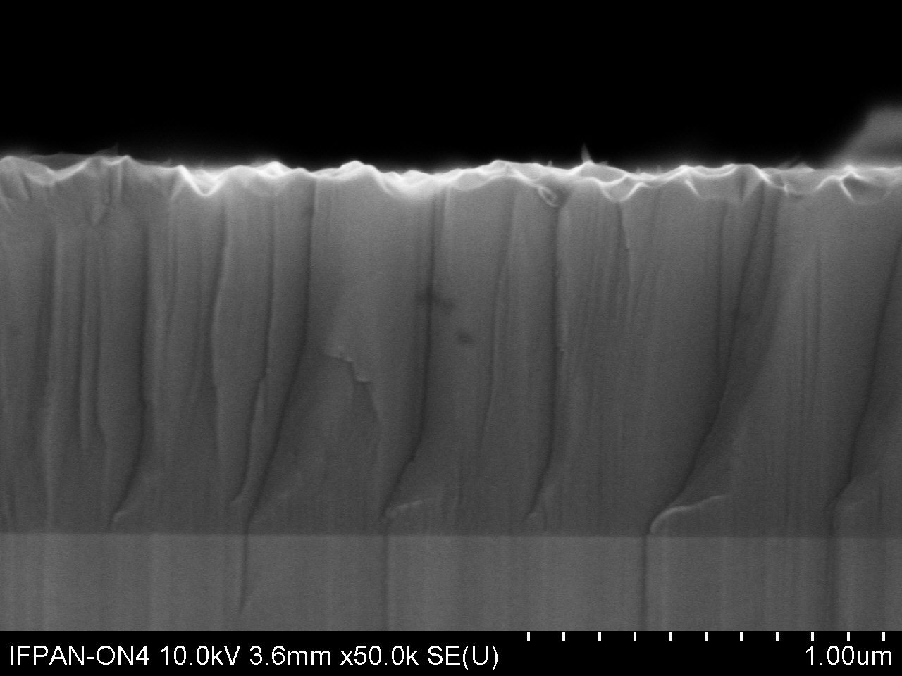
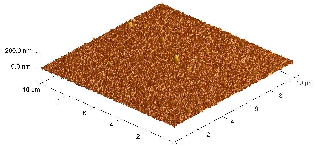
DescriptionThin films of zinc oxide (ZnO) are obtained by atomic layer deposition (ALD) on gallium nitride (GaN) substrates. The material is formed in a double exchange chemical reaction between two reactants (precursors), such as a deionized water (oxygen precursor) and a diethylzinc - DEZ (zinc precursor). ZnO can be grown at the temperature range from 250°C to 300°C. The maximum size of the substrate is 20 cm of a diameter.
Specification
ApplicationsZnO and GaN are two semiconductor materials, which are investigated for many possible applications in electronics, optoelectronics, biology, and medicine. Physical and chemical properties of both GaN and ZnO mean that these materials can be used as light emitting diodes (LEDs), sensor devices, in transparent electronics, and in solar cells. Short-wavelength UV detectors based on n-GaN/p-GaN homojunctions have been widely studied. Despite the fact that GaN-based LEDs, laser diodes and detectors are commercialized, some of their properties need further improvements. In particular, our fi rst investigations show that ZnO-based UV detectors can not only be more sensitive, but also much cheaper than the ones based on GaN.
Patent application: P.395334 (27-06-2011) |
| |||