
Transmission Electron Microscopy (TEM) | ||||
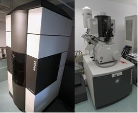
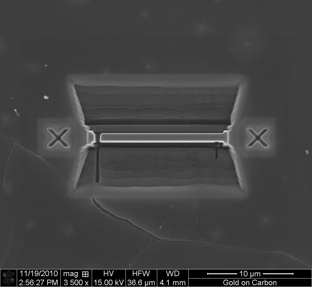
DescriptionIn the Laboratory of Electron Microscopy (PME), the structure and chemical composition of solids are investigated. The Laboratory is equipped with a transmission electron microscope FEI Titan 80-300 Cubed and a dual beam scanning microscope Helios-NanoLab. The Helios-NanoLab 600 is used for FIB sample preparation for transmission electron microscopy as well as for other tasks such as the determining the elemental composition of samples (EDXS) or nanolithography by focused gallium ions beam (FIB). PME performs two test procedures covered by the accreditation of the PCA. Methods
Parameters
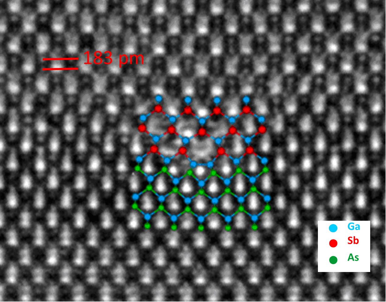
Investigated materialssemiconductor epitaxial heterostructures (GaN, Si, Ga(Mn)As, CdZnTe, SnPbTe, SiC on Si), materials for spinelectronics ((Ga, Mn)Sb, (Cu, Co)ZnO, (Cd, Zn, Mn, Mg)Te, (Mg,Zn)Se), nanowires (ZnTe, ZnTe/CdTe, GaAs, (In, Mn)GaAs, SnPbTe), nonoparticles (ZnO, Ag, Au, Pd, Pt, Fe2O3, Fe3O4), biological materials.
|
| |||